DS2409 Emulation
To emulate a DS2409 one needs 1-Wire addressable switches (for digital control and sensing) and analog switches (to activate or deactivate the outputs). A partial emulation is possible with a 2-channel addressable switch (e.g., DS2413, DS2406, or DS28E04) plus one or two analog switches. For a full emulation one needs a 5-channel 1-Wire addressable switch (e.g., DS2408, 8 channels) plus two analog switches. It is important that the addressable switch powers up with all PIOs in an off (nonconducting) state.
The analog switch must be of the single-pole/double-throw (SPDT) type. When selecting a switch, look for a supply voltage of 5V ±10%, an on-resistance (RON) of 30Ω or less, and low capacitance (no more than 50pF) on all three nodes of the switch. The turn-on and turn-off time should not exceed 100ns. Excellent built-in ESD protection is desirable. Based on data sheet specifications, the following analog switches were identified as suitable:
- Single-channel: MAX4729 (5.7Ω, max), MAX4730 (5.7Ω, max), MAX4644 (4.75Ω, max)
- Dual-channel: MAX4717 (3.5Ω, max), MAX4719 (25Ω, max), MAX4635 (4.5Ω, max), MAX4636 (4.5Ω, max), MAX4750 (30Ω, max)
- Triple-channel: MAX4693 (25Ω, typical, 40Ω, max; slow switching).
None of the above switches has good ESD protection. The bench tests were conducted using the MAX4561 single-channel switch, which has built-in ESD protection of ±15kV at the NO and NC pins. Particularly due to its high RON value of typically 45Ω, the MAX4561 should not be considered for DS2409 emulation.
Example Circuits
The example circuit in Figure 7 is a partial emulation that implements one switched 1-Wire output and the control output of the DS2409. U1 is the 2-channel 1-Wire addressable switch with open-drain PIO ports. U2 is the SPDT analog switch. The three switch terminals occupy pins NO, NC, and COM. The switch is controlled by the digital level at the IN pin.
In the power-on default state, both PIOs of the 1-Wire addressable switch are in high impedance. Resistor R2 applies a logic-high to the switch's IN pin, which causes the NO pin to be connected to COM. Resistor R1 at the NO pin provides the 1.5kΩ pullup to the inactive 1-Wire output at the COM pin. This is equivalent to the power-on state of the DS2409.
To activate the 1-Wire output of U2, the master turns PIO-A on, which applies a logic-low to the IN pin of U2. This causes the analog switch to disconnect COM from NO and to connect it to NC, i.e., the incoming 1-Wire bus. Turning PIO-A off deactivates the 1-Wire output. The master can operate PIO-B independently of PIO-A, e.g., to emulate the DS2409's control output in manual mode or to control another R1/R2/U2-like circuit. When controlling two analog switches, the 1-Wire master must ensure that no more than one 1-Wire output is activated. This can be done through software or (safer) with the help of glue logic that decodes the cases PIO-A ^ active-low PIO-B and active-low PIO-A ^ PIO-B to control the analog switches. PIO-B could also be used for event detection (conditional search) and short detection (dotted line). A reset pulse before output activation cannot be supported.
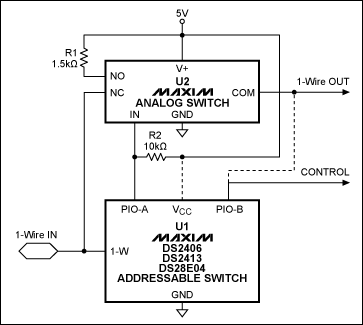
Figure 7. Partial DS2409 emulation circuit . U1 could be a DS2406, DS2413 or DS28E04.
DS2406 Addressable Switch
The circuit of Figure 7 has been tested using the DS2406 addressable switch. The IN pin of the analog switch (MAX4561) was connected to PIO-B of the DS2406. PIO-A was used as a control output to turn on an LED. The PIOs were operated using the Write Status command (code 55h), addressing memory location 0007h (SRAM control bits). Bit 6 of the SRAM control bits directly accesses the PIO-B channel flip flop. Figure 8 shows the output activation sequence. Visible in the top trace are the CRC16 bytes (1Fh, E2h) that follow the 3Fh data byte that was written to address 0007h. The bottom trace shows the PIO-B transition, which controls the analog switch. There is no activity on the 1-Wire output (center trace) until the reset/ PD cycle that follows immediately after the CRC16. This reset/PD is not included in Figure 8.
Figure 9 shows the output deactivation sequence. Visible in the top trace are the CRC16 bytes (1Eh, 12h) that follow the 7Fh data byte that was written to address 0007h. The bottom trace shows the PIO-B transition, which controls the analog switch. Activity on the 1-Wire output (center trace) ends with the state change at PIO-B, after which the master issues a reset/PD cycle. This reset/PD is not included in Figure 9.
Instead of writing to the Status register, the PIOs can also be controlled using the Channel Access command (code F5h). This, however, was not attempted. Also, note that the DS2406 performs a power-on reset after less than 1 minute without power. The DS2409, in contrast, undergoes a power-on reset cycle if the supply voltage was interrupted or if the 1-Wire input was disconnected (low) for only a few milliseconds. The DS2406 has activity latches at its PIOs. Therefore, it can support event detection (conditional search) and short detection (dotted line). The activity latches are cleared through the Channel Access command (channel control byte 1).
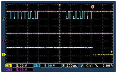
Figure 8. Partial emulation with DS2406, output activation.

Figure 9. Partial emulation with DS2406, output deactivation.
 電子發燒友App









評論