USB powered devices must meet certain specifications. The input capacitance must be less than 10uF to minimize inrush current, and subsequently must draw less than 100mA before given permission from the USB controller to draw up to 500mA. For most applications these requirements can be met by using less than 10uF for the input capacitor to meet the inrush current, and an enable signal that interfaces with the USB controller and turns on the unit, allowing it to draw current up to 500mA.
For dying gasp applications, there must be a local energy storage capacitor that will power the device and prolong its operation for orderly shut down when USB power is lost. The loss of USB power is sensed and a warning signal is issued. To meet the dying gasp warning time, the energy storage capacitor value needed is much larger than the 10uF allowed. The circuit in Figure 1 is designed to solve this problem.

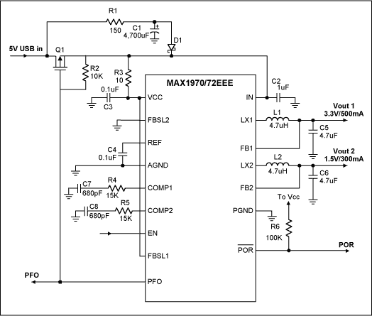
Figure 1. Typical application circuit for 5V USB dying gasp application.
Even though C1 can be thousands of uF, its charging current is limited by R1 to 33mA. The only inrush current is the charging current of C2 via the body diode of Q1. However, C2 is only 1uF, much smaller than that allowed by USB specifications.
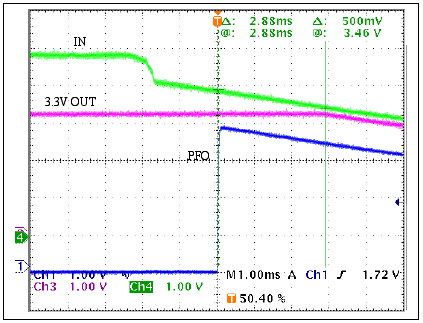
Under normal operation, input current to the MAX1970 flows through Q1, and C1 is charged to ~5V USB in. When the 5V USB power fails or turns off, the energy stored in C1 provides power via D2. As C1 discharges to the MAX1970 input power fail (PFO) threshold of 3.94V, PFO goes high to turn off Q1, and issues an input power warning while both outputs are still in regulation. C1 continues to discharge and the higher output voltage (3.3V) drops out. The power fail warning time is measured from the time PFO goes high to the time when the 3.3V output drops out of regulation. Figure 2 shows the typical PFO warning time of 2.88mS for the circuit in Figure 1, when 3.3V and 1.5V are loaded at 500mA and 300mA respectively.

Figure 2. Input power fail (PFO) warning time.
The top trace in Figure 2 is the voltage at the MAX1970 IN pin. As the 5V USB input is turned off and the storage capacitor C1 starts to supply the energy to the DC/DC converter, the voltage at the IN pin drops, due to forward voltage of D1. As C1 continues to discharge to the PFO threshold, PFO goes high and turns off Q1. C1 further discharges until the 3.3V output starts to droop, when IN is about 3.5V.
The PFO warning time depends on the value of C1, the output voltages and load currents, as well as the DC/DC converter efficiency. The input power required, which must be supplied from C1 during the warning time, is:
Pin = (1/n) × ((Vout1 × Iout1) + (Vout2 × Iout2))where n is the converter efficiency.
Since the regulated DC/DC converter is a constant power load, as the voltage IN pin decreases the current increases to maintain constant power. When PFO goes high, this voltage is at ~3.94V and starts decaying to drop-out at ~3.5V. The average current supplied from C1 can be calculated as:
Ic avg = 1/2 × Pin × (1/3.94 + 1/3.5)The time it takes for C1 to discharge a differential voltage of 0.44V (3.94V–3.5V), is the PFO warning time. This time can be calculated as:
Twarn = (0.44V × C1)/ Ic avg.To ensure for worst-case component tolerances, such as capacitance of C1, DC/DC converter efficiency, PFO threshold, and temperature, it is recommended to size the capacitor C1 to twice the value calculated for the minimum warning time required.
For the circuit in Figure 1, when 3.3V and 1.5V are loaded at 500mA and 300mA respectively, the input power calculated by equation (1) is 2.33Watts at n = 90%. The average current supplied from C1 as calculated by equation (2) is 628mA. Finally, the warning time calculated by equation (3) is 3.28mS, which agrees with the oscilloscope plot of Figure 2 to within the 20% tolerance of C1.
 電子發(fā)燒友App


評論