Abstract: Canceling the load allows the op amp the capability for high output current while maintaining all the other high-accuracy specifications such as very high open-loop gain, low offset voltage and current, low offset-voltage and offset-current noise, and low distortion.
Accurate op amps are often characterized as having very high open-loop gain, low offset voltage and current, low offset-voltage and offset-current noise, and low distortion. Conspicuously absent is the capability for high output current while maintaining all the other high-accuracy specifications. Thus, high-accuracy op amps have a problem driving low-impedance loads.
One solution is to "cancel" the load. If your resistive load is "R"Ω and you connect in parallel with it a negative resistor of "-R"Ω, resistance of the parallel combination is infinite. Negative resistance can be generated as shown in the circuit of Figure 1: Rin = -Rnf(R1/R2). This quantity is derived as follows: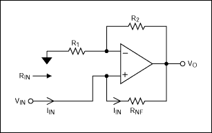
Figure 1. This circuit produces a negative resistance of Rin = -Rnf(R1/R2).
Figure 2 presents a practical application of the concept. The first op amp is an accurate unity-gain buffer, and the second op amp is a high-current, wide-bandwidth, gain-of-2 driver. Because R1 = R2 in this negative-resistor stage, its input resistance is -Rnf = -200Ω, which matches the magnitude of the accurate buffer's 200Ω load resistance. If these magnitudes were perfectly matched, the buffer would see an (almost) open circuit.
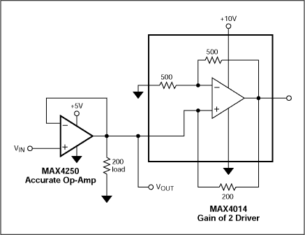
Figure 2. Connecting a load-cancelling negative resistor in parallel with the load of a precision op amp enables that op amp to drive 200Ω.
The buffer drives the positive input of the second amplifier, and the second amplifier drives the load. Gain error, output-current limits, and resistor mismatches limit the minimum resistance that can be driven, but driving a 200Ω load is easy. That load is an order of magnitude lower than the accurate amplifier can otherwise handle without suffering some loss of performance.
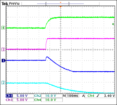
Note that the first op amp's accuracy (to first order) is not affected by the second op amp's gain error, offset voltage, and offset current. Nor does the driver have significant positive feedback, because its positive input is driven by the extremely low output impedance of the first op amp. The step response of this circuit is very well behaved and exhibits no ringing.
The negative-resistance approach works equally well with dual-supply op amps, because the negative-resistor portion can both source and sink current. If the driver op amp does not have built-in gain-setting resistors, its non-inverting gain may be set closer to unity, thereby (perhaps) allowing both op amps to share the same power supply. This approach limits the output swing of the accurate op amp, but that restriction may be acceptable in a given application. To guarantee full bandwidth for the accurate op amp, the driver op amp should have much wider bandwidth.
A similar version of this article appeared in the May 24, 2001 issue of EDN magazine.
Accurate op amps are often characterized as having very high open-loop gain, low offset voltage and current, low offset-voltage and offset-current noise, and low distortion. Conspicuously absent is the capability for high output current while maintaining all the other high-accuracy specifications. Thus, high-accuracy op amps have a problem driving low-impedance loads.
One solution is to "cancel" the load. If your resistive load is "R"Ω and you connect in parallel with it a negative resistor of "-R"Ω, resistance of the parallel combination is infinite. Negative resistance can be generated as shown in the circuit of Figure 1: Rin = -Rnf(R1/R2). This quantity is derived as follows:
Vo = Vin(1 + R2/R1)
Iin = (Vin - Vo)/Rnf = -(Vin/Rnf)(R2/R1)
Rin = Vin/Iin = -Rnf(R1/R2).

Figure 1. This circuit produces a negative resistance of Rin = -Rnf(R1/R2).
Figure 2 presents a practical application of the concept. The first op amp is an accurate unity-gain buffer, and the second op amp is a high-current, wide-bandwidth, gain-of-2 driver. Because R1 = R2 in this negative-resistor stage, its input resistance is -Rnf = -200Ω, which matches the magnitude of the accurate buffer's 200Ω load resistance. If these magnitudes were perfectly matched, the buffer would see an (almost) open circuit.

Figure 2. Connecting a load-cancelling negative resistor in parallel with the load of a precision op amp enables that op amp to drive 200Ω.
The buffer drives the positive input of the second amplifier, and the second amplifier drives the load. Gain error, output-current limits, and resistor mismatches limit the minimum resistance that can be driven, but driving a 200Ω load is easy. That load is an order of magnitude lower than the accurate amplifier can otherwise handle without suffering some loss of performance.
Note that the first op amp's accuracy (to first order) is not affected by the second op amp's gain error, offset voltage, and offset current. Nor does the driver have significant positive feedback, because its positive input is driven by the extremely low output impedance of the first op amp. The step response of this circuit is very well behaved and exhibits no ringing.
The negative-resistance approach works equally well with dual-supply op amps, because the negative-resistor portion can both source and sink current. If the driver op amp does not have built-in gain-setting resistors, its non-inverting gain may be set closer to unity, thereby (perhaps) allowing both op amps to share the same power supply. This approach limits the output swing of the accurate op amp, but that restriction may be acceptable in a given application. To guarantee full bandwidth for the accurate op amp, the driver op amp should have much wider bandwidth.
A similar version of this article appeared in the May 24, 2001 issue of EDN magazine.
 電子發燒友App









評論