Abstract: Described circuit provides a thermal output from a piezofilm transducer. The circuit is a high-input-impedance differential charge amplifier using three op amps in a somewhat classical instrumentation amplifier configuration. The differential stage rejects resistor-generated thermal noise, and acts as a first-order high-pass filter. Choice of component values is discussed, and some typical valuese are suggested. Alternate configurations are suggested for overcoming some typical circuit limitations.
Piezoelectric films (piezofilms, or piezo-films) can convert signals in a variety of ways: electrical to mechanical (e.g., a loudspeaker), mechanical to electrical (microphone), and thermal to electrical (temperature sensor). In the circuit of Figure 1, the piezofilm element performs thermal to electrical and mechanical to electrical conversions. It is intended to act as a temperature sensor and only incidentally acts as a microphone.
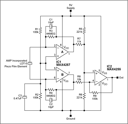
Figure 1. This amplifier is designed to extract the piezofilm sensor's thermal signal.
The electrical analog of a piezofilm sensor is a capacitor in series with a voltage source. The sensor has high output impedance and requires a high-impedance buffer amplifier. The circuit shown includes a differential charge amplifier followed by a differential-to-single-ended amplifier. The differential topology reduces line-noise pickup, which is a problem in high-gain circuits.
A dual op amp (IC1) endows the differential charge amplifier with single-supply operation and low supply current. R1, R2, and a small bypass capacitor (C3) set the input common-mode voltage at the mid-supply level.
Thermal noise generated by these resistors is not amplified by the differential amplifier. Instead, it appears as a common-mode signal at the differential outputs and is attenuated by common-mode rejection in the following stage. Because thermal noise is proportional to resistance, this topology-by not amplifying biasing noise-offers the advantage of lower supply current for a given noise target.
AC gain for the differential stage is set by the C1 and C2 value relative to the sensor capacitance (CEQ). In this case, CEQ measures 484pF at 1kHz, with an equivalent series resistance (ESR) of 5kΩ. You can model the sensor as a differential voltage source in series with two capacitors of value 2CEQ. R3 and R4 have little effect at high frequencies because feedback is dominated by the reactance of C1 and C2. As a result, each half of the circuit has a gain of C1/CEQ = 96.
The differential amplifier also acts as a first-order high-pass filter. To simplify analysis, let C1=C2=C and R3=R4=R. Then, an inspection of either half of the amplifier shows a pole at 1/2πRC and a gain of CEQ/C at infinite frequency. AC gain is proportional to CEQ/C, so high AC gain implies a small C. In this case C = 10pF and R = 44MΩ, which leads to a corner frequency of 360Hz. R must be very large for good low-frequency response. Lowering the corner frequency means increasing the value of R, but the op amp's input leakage flowing in a large feedback resistor can produce a large offset voltage. To counter this effect, the dual op amp shown is a CMOS device chosen for its small input leakage, which is only 1pA.
Differential-to-single-ended conversion is performed by IC2 and the resistors R5, R6, R8, and R9. The values shown give a differential gain of 20.
Line-noise rejection depends on the match between C1 and C2, but tight-tolerance capacitors are expensive (in general, this is a disadvantage of differential charge amplifiers). If you can't obtain a perfect match, however, the circuit's first-order rejection is still better than that of a single-ended amplifier.
The incorporation of gain in a differential-to-single-ended converter degrades common-mode rejection. To avoid this problem, you can replace the differential-to-single-ended circuit with a unity-gain differential-to-single-ended converter and another single-ended gain stage.
A scope display (Figure 2) demonstrates the pyro-electrical (heat sensing) capability of this circuit. The dip in the trace is caused by a heated soldering iron that moved quickly past the sensor at a distance of about six inches. The sensor's acoustic pickup produces the smaller signals riding on this trace. They can be canceled by adding a replica circuit that responds to the same ambient acoustical noise but not to the heat.
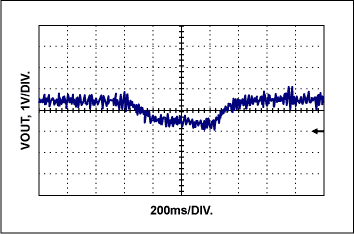
Figure 2. A soldering iron passing about six inches from the sensor in Figure 1 caused this dip in the circuit's output trace.
If you want to construct this circuit using a dual op amp with a smaller package, consider the MAX4252 and MAX4253. Both these devices come in an ultra chip-scale package (UCSP). They are identical, except the MAX4253 allows individual shutdown of each of the two op amps contained within its package. These devices are unity-gain stable with an open-loop gain of 3MHz, and should work in this circuit despite the difference in bandwidth between them and the op amps shown in Figure 1. Note, however, that the circuit has not been tested with either the MAX4252 or the MAX4253, but instead with the op amps pictured in Figure 1.
Piezoelectric films (piezofilms, or piezo-films) can convert signals in a variety of ways: electrical to mechanical (e.g., a loudspeaker), mechanical to electrical (microphone), and thermal to electrical (temperature sensor). In the circuit of Figure 1, the piezofilm element performs thermal to electrical and mechanical to electrical conversions. It is intended to act as a temperature sensor and only incidentally acts as a microphone.
Figure 1. This amplifier is designed to extract the piezofilm sensor's thermal signal.
The electrical analog of a piezofilm sensor is a capacitor in series with a voltage source. The sensor has high output impedance and requires a high-impedance buffer amplifier. The circuit shown includes a differential charge amplifier followed by a differential-to-single-ended amplifier. The differential topology reduces line-noise pickup, which is a problem in high-gain circuits.
A dual op amp (IC1) endows the differential charge amplifier with single-supply operation and low supply current. R1, R2, and a small bypass capacitor (C3) set the input common-mode voltage at the mid-supply level.
Thermal noise generated by these resistors is not amplified by the differential amplifier. Instead, it appears as a common-mode signal at the differential outputs and is attenuated by common-mode rejection in the following stage. Because thermal noise is proportional to resistance, this topology-by not amplifying biasing noise-offers the advantage of lower supply current for a given noise target.
AC gain for the differential stage is set by the C1 and C2 value relative to the sensor capacitance (CEQ). In this case, CEQ measures 484pF at 1kHz, with an equivalent series resistance (ESR) of 5kΩ. You can model the sensor as a differential voltage source in series with two capacitors of value 2CEQ. R3 and R4 have little effect at high frequencies because feedback is dominated by the reactance of C1 and C2. As a result, each half of the circuit has a gain of C1/CEQ = 96.
The differential amplifier also acts as a first-order high-pass filter. To simplify analysis, let C1=C2=C and R3=R4=R. Then, an inspection of either half of the amplifier shows a pole at 1/2πRC and a gain of CEQ/C at infinite frequency. AC gain is proportional to CEQ/C, so high AC gain implies a small C. In this case C = 10pF and R = 44MΩ, which leads to a corner frequency of 360Hz. R must be very large for good low-frequency response. Lowering the corner frequency means increasing the value of R, but the op amp's input leakage flowing in a large feedback resistor can produce a large offset voltage. To counter this effect, the dual op amp shown is a CMOS device chosen for its small input leakage, which is only 1pA.
Differential-to-single-ended conversion is performed by IC2 and the resistors R5, R6, R8, and R9. The values shown give a differential gain of 20.
Line-noise rejection depends on the match between C1 and C2, but tight-tolerance capacitors are expensive (in general, this is a disadvantage of differential charge amplifiers). If you can't obtain a perfect match, however, the circuit's first-order rejection is still better than that of a single-ended amplifier.
The incorporation of gain in a differential-to-single-ended converter degrades common-mode rejection. To avoid this problem, you can replace the differential-to-single-ended circuit with a unity-gain differential-to-single-ended converter and another single-ended gain stage.
A scope display (Figure 2) demonstrates the pyro-electrical (heat sensing) capability of this circuit. The dip in the trace is caused by a heated soldering iron that moved quickly past the sensor at a distance of about six inches. The sensor's acoustic pickup produces the smaller signals riding on this trace. They can be canceled by adding a replica circuit that responds to the same ambient acoustical noise but not to the heat.
Figure 2. A soldering iron passing about six inches from the sensor in Figure 1 caused this dip in the circuit's output trace.
If you want to construct this circuit using a dual op amp with a smaller package, consider the MAX4252 and MAX4253. Both these devices come in an ultra chip-scale package (UCSP). They are identical, except the MAX4253 allows individual shutdown of each of the two op amps contained within its package. These devices are unity-gain stable with an open-loop gain of 3MHz, and should work in this circuit despite the difference in bandwidth between them and the op amps shown in Figure 1. Note, however, that the circuit has not been tested with either the MAX4252 or the MAX4253, but instead with the op amps pictured in Figure 1.
評論
查看更多