電路能力測試-3:影像信號放大電路
Circuit Knowledge Test-3: Video Buffer
 ?
?
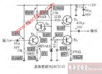
1. If video input voltage is 1 Vpp, what will be video voltage at QV2 collector and QV1 collector? (Line output with or without 75 ohm load)
影像信號輸入為1V峰對峰值,計算QV2及QV1集極信號電壓值。(包括輸出端有無75 Ohm負載)
?
2. How to check video output waveform in order to make sure the video buffer circuit is working properly? (Hint: most common happened clamped video and tilted sync defects)
如何以儀器確認影像信號經過放大以后,輸出波形為正常。(一般會有上下波幅切割或是同步信號扭曲問題)
?
3. Which components are needed to be value-changed for the adjustments of QV1 and QV2 collector bias? How to adjust for top side or bottom side clamped video?
那些元件是用來調整QV2及QV1的集極電壓,以避免輸出信號的上下切割問題。問題發生時,元件數值應該如何改變處理。
?
4. Plot the waveform for a regular pulse and pulses on
繪出下列五種波形:標準脈波,低頻不足的脈波,高頻不足的脈波,過沖震蕩脈波,下沖震蕩脈波。
?
試題解答
Circuit Knowledge Test-3: Video Buffer
ANS-1:
Buffer gain Av for QV2 = RV4/RV7 = 1.8?
Buffer gain Av for QV1 = RV9/RV2 = 1.8 (without 75 Ohm load)
While QV2 load will change to 43 Ohm with 75 Ohm load. RV9/RV2 = 0.8
Video voltage at QV2 is 1.8 Vpp, at QV1 is 3.2 Vpp without load and 1.4 Vpp with load.
?
ANS-2:
Utilize gray scale pattern video signal with H-sync sweep scope setting to check clamped video defect.
Correct percentage of sync level must be 30% to show no clamped video defect.
?
Utilize full white pattern video signal with V-sync sweep scope setting to check tilted sync defect.
No tilted V-sync pulse and no tilted peak white are allowed.
?
ANS-3:
RV3 is suitable for adjusting QV2 bias, while RV8 is suitable for adjusting QV1 bias.
Increase RV3 value or reduce RV8 value for modified bottom side clamped video.
Reduce RV3 value or increase RV8 value for modified top side clamped video.
?
ANS-4:
 ?
?
 電子發燒友App









評論