This unique solution features Altera's low-cost Cyclone? III or Cyclone IV FPGAs and intellectual property from Eyelytics and Apical supporting AltaSens' 1080p60 A3372E3-4T and Aptina's 720p60 MT9M033 HD Wide Dynamic Range (WDR) CMOS image sensors. The all-in-one solution offers surveillance equipment manufacturers the ability to reduce board space, lower power consumption, increase flexibility and reduce development time compared to previous architectures using traditional digital signal processors and ASSPs.
Traditional digital signal processors and ASSPs don't have the processing power required to accept the large bandwidth of data from 1080p and 720p WDR CMOS sensors (for instance, a full HD raster is 2200x1125 pixels x 16+ bits per pixel x 60 frames per second, resulting in >2 Gbps bandwidth). Altera's Cyclone series FPGAs deliver the bandwidth and processing performance needed, handling large amounts of data generated by today's HD WDR CMOS image sensors. In previous designs, HD WDR camera systems required FPGAs to perform the “front end” data processing while a digital signal processor or an ASSP handled the “back end” video encoding. Now, all of these chips can be replaced by a single Altera? FPGA.
The functions of Altera's HD surveillance IP camera reference design include:
Apical's ISP incorporating best-in-class WDR processing “iridix” together with advanced temporal and spatial noise reduction Apical's “checkerboard demosaic” core for the Altasens A3372E3-4T WDR mode “3A” functions, such as auto exposure and auto white balance implemented in software on Altera's Nios? II embedded soft core processor Eyelytics' H.264 video encoder, capable of 720-line progressive 30 frames-per-second encoding or 1080-line progressive 15 frames-per-second encoding in main profile Altera's triple-speed Ethernet MAC intellectual property core
圖1。參考設(shè)計(jì)外形圖
一.Next-Generation, Megapixel WDR Image Sensor MT9M033
Best-In-Class, HD Video Sensor
Providing 720p at 60 fps HD streaming, this image sensor offers high-speed video performance.
Superior, Low-Light Performance
Dynamic pixel response technology significantly improves sensitivity for superb low-light performance.
Exceptional Image Quality
The MT9M033 has a dynamic range of up to 120dB, producing crystal-clear images in all lighting conditions.
Perfect for Day/Night Camera Applications
High quantum efficiency in visible/NIR range improves versatility for use in day and night applications.
All-Purpose Image Solution
The perfect choice for mainstream surveillance lens formats.
MT9M033主要特性:
? Best-in-class, low-light performance
? HD video (60 fps @ 720p)
? Linear or high dynamic range video streaming
? Video and snapshot modes
? 2X2 binning and windowing
? Flexible row-skip modes
? Parallel and serial ouputs
? On-chip AE and statistics engine
? Support for external LED or flash
? Auto black level calibration
? Context switching
? Sophisticated camera functions, including auto exposure control, windowing, binning, and high-speed row-skipping mode
? Programmable through two-wire serial interface
? Advance gain control
MT9M033技術(shù)指標(biāo):
? Imaging Array
? Optical Format: 1/3-inch
? Active Array: 1280(H) x 960(V)
? Imaging Area: 3.54mm(H) x 2.69mm(V) Speed/Output
? Frame Rate: 60 fps @ 720p (HD mode); 45 fps @ full resolution
? Data Rate: 27 Mb/s
? Master Clock: 74.25 MHz
? Data Format: Serial (HiSPi), parallel (12- or 14-bit)Sensitivity
? Pixel Size: 3.75μm x 3.75μm
? Pixel Dynamic Range: 120dB
? Responsivity: 6.0 V/lux-sec Power
? Supply: I/O: 1.8V
Core: 1.8V
Analog: 2.8V
? Consumption: ~300mW
Temperature Range
? Operating: –20°C to +70°C
? Storage: –40°C to +125°C
Package: iLCC or die
MT9M033應(yīng)用:
? Surveillance cameras
? Automatic license plate recognition (ALPR) cameras
? Wide dynamic range (WDR) cameras
? HDTV
? Day/Night cameras
? Dome cameras
? Pan, tilt, zoom cameras

圖2。MT9M033方框圖
二.Cyclone? III開發(fā)板
The Cyclone? III development board provides a hardware platform for developing and prototyping low-power, high-volume, feature-rich designs as well as to demonstrate the Cyclone III device's on-chip memory, embedded multipliers, and the Nios? II embedded soft processor.
With up to 4-Mbits of embedded memory and 288 embedded 18-bit x 18-bit multipliers, the Cyclone III device supplies an abundance of internal memory while also providing external support for high-speed, low-latency memory access via dual-channel DDR SDRAM and low-power SRAM.
Built on TSMC's 65-nm low-power process technology, Cyclone III devices are designed to provide low static and dynamic power consumption. Additionally, with the support of the Quartus? II software's PowerPlay technology, designs are automatically optimized for power consumption. Therefore, the Cyclone III development board provides a power-optimized, integrated solution for memory-intensive, high-volume applications.
Accordingly, the Cyclone III development board is especially suitable for wireless, video and image processing, and other high-bandwidth, parallel processing applications. Through the use of Altera?-provided video and image intellectual property (or other MegaCore? functions) and board expansion connectors, you can enable the inter-operability of the Cyclone III device, allowing application-specific customization of the development board.
The Cyclone III development board has the following main features:
■ Higher logic density to implement more functions and features
■ More embedded memory for high-bandwidth applications
■ Expandable through two Altera High Speed Mezzanine Card (HSMC) connectors
■ 256-MB of dual channel DDR2 SDRAM with a 72-bit data width
■ Supports high-speed external memory interfaces including dual-channel DDR SDRAM and low-power SRAM
■ Four user push-button switches
■ Eight user LEDs
■ Power consumption display
The Cyclone III development board provides the following advantages:
■ Unique combination of low-cost, low-power Cyclone III FPGA that supports high-volume, memory-intensive designs
■ Highest multiplier-to-logic ratio FPGA in the industry
■ Lowest cost, density- and power-optimized FPGA
■ Quartus II development software's power optimization tools
The board features the following major component blocks:
■ 780-pin Altera Cyclone III EP3C120 FPGA in a BGA package
● 119K logic elements (LEs)
● 3,888 Kbits of memory
● 288 18 x 18 multiplier blocks
● Four phase locked loops (PLLs)
● 20 global clock networks
● 531 user I/Os
● 1.2 V core power
■ 256-pin Altera MAX? II EPM2210G CPLD in a FineLine Ball Grid Array (FBGA) package
● 1.8 V core power
■ On-board memory
● 256 MB dual-channel DDR2 SDRAM
● 8 MB SRAM
● 64 MB flash memory
■ FPGA configuration circuitry
● MAX II CPLD and flash passive serial configuration
● On-board USB-Blaster? circuitry using the Quartus II Programmer
■ On-board clocking circuitry
● Two clock oscillators to support Cyclone III device user logic
? 50-MHz
? 125-MHz
● 80 I/O, 6 clocks, SMBus, and JTAG
● SMA connector for external clock input and output
■ General user and configuration interfaces
● LEDs/displays:
? Eight user LEDs
? One transmit/receive LED (TX/RX) per HSMC interface
? One configuration done LED
? Ethernet LEDs
? User 7-segment display
? Power consumption display
● Memory activity LEDs:
? SRAM
? FLASH
? DDR2 Top
? DDR2 Bottom
● Push-buttons:
? One user reset push-button (CPU reset)
? Four general user push-buttons
? One system reset push-button (user configuration)
? One factory push-button switch (factory configuration)
● DIP switches:
? One MAX control DIP switch
? One JTAG control switch
? Eight user DIP switches
● Speaker header
■ Displays
● 128 x 64 graphics LCD
● 16 x 2 line character LCD
■ Power supply
● 14 V - 20 V DC input
● On-board power measurement circuitry
● Up to 19.8 W per HSMC interface
■ Mechanical
● 6”x 8” board
● Bench-top design
Cyclone III EP3C120開發(fā)板
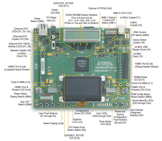
圖3。Cyclone III EP3C120開發(fā)板外形圖
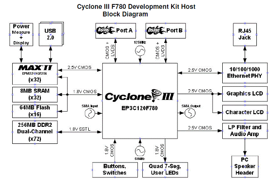
圖4。Cyclone III EP3C120開發(fā)板方框圖
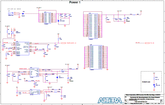
圖5。Cyclone III EP3C120開發(fā)板電路圖(1)

圖6。Cyclone III EP3C120開發(fā)板電路圖(2)

圖7。Cyclone III EP3C120開發(fā)板電路圖(3)
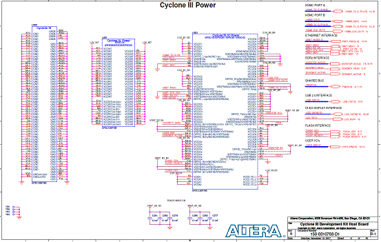
圖8。Cyclone III EP3C120開發(fā)板電路圖(4)
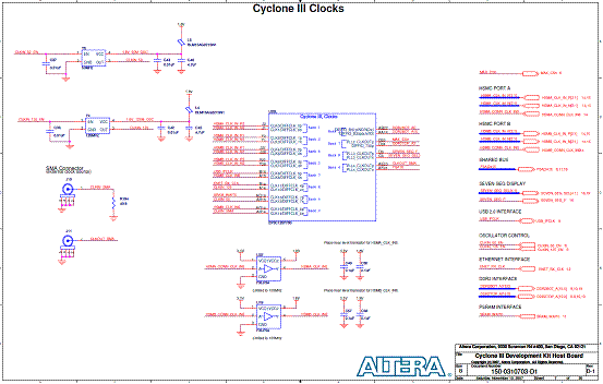
圖9。Cyclone III EP3C120開發(fā)板電路圖(5)
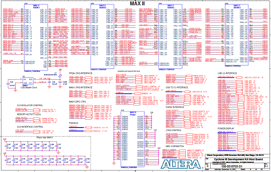
圖10。Cyclone III EP3C120開發(fā)板電路圖(6)
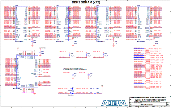
圖11。Cyclone III EP3C120開發(fā)板電路圖(7)

圖12。Cyclone III EP3C120開發(fā)板電路圖(8)
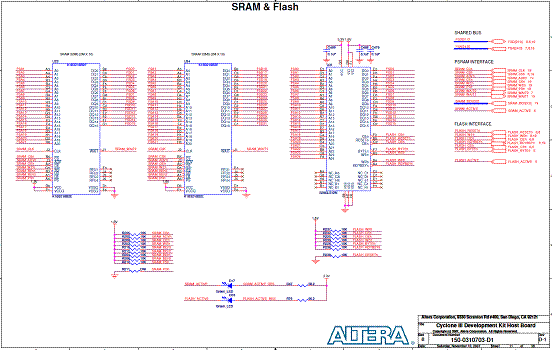
圖13。Cyclone III EP3C120開發(fā)板電路圖(9)
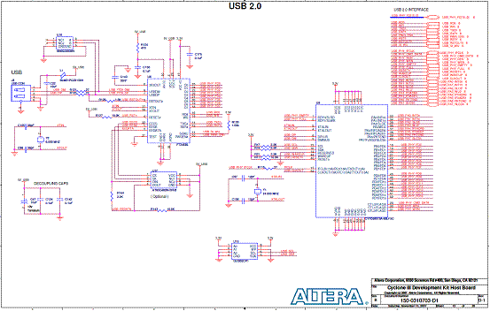
圖14。Cyclone III EP3C120開發(fā)板電路圖(10)
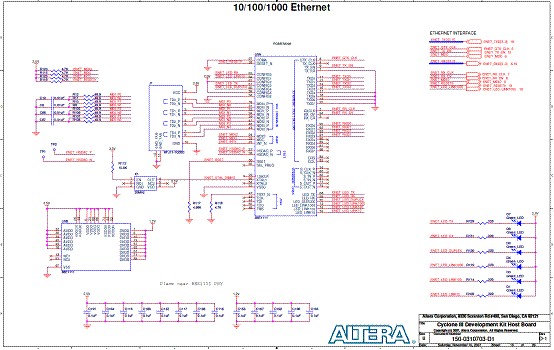
圖15。Cyclone III EP3C120開發(fā)板電路圖(11)
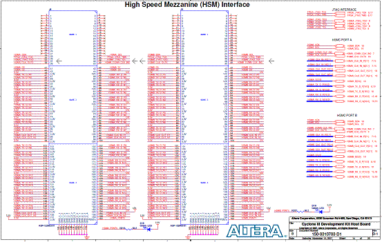
圖16。Cyclone III EP3C120開發(fā)板電路圖(12)

圖17。Cyclone III EP3C120開發(fā)板電路圖(13)
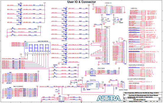
圖18。Cyclone III EP3C120開發(fā)板電路圖(14)

圖19。Cyclone III EP3C120開發(fā)板電路圖(15)
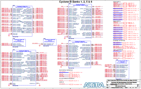
圖20。Cyclone III EP3C120開發(fā)板電路圖(16)
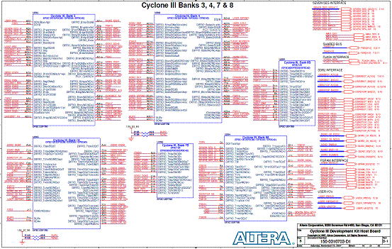
圖21。Cyclone III EP3C120開發(fā)板電路圖(17)
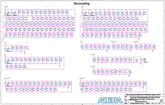
圖22。Cyclone III EP3C120開發(fā)板電路圖(18)
The Bitec HSMC DVI interface card is designed to allow developers access to high-quality, high resolution video signals in their FPGA designs. It integrates both a DVI receiver and transmitter onto the same card giving the flexibility required by high resolution image processing systems. The latest release hosts both TX and RX Optical S-PDIF interfaces for up to 15Mbps digital audio. Card is shipped with source code examples.
Bitec DVI HSMC接口板特性:
??Digital Visual Interface Compliant (DVI 1.0)
??Supports resolutions from VGA to UXGA (1600x1200 & 1920x1080)
??25 – 165 Mhz Pixel rates
??EDID data reading/writing
??Monitor detection through Hot-Plug
??S-PDIF Optical Tx and Rx
Bitec DVI HSMC接口板應(yīng)用:
??Machine vision
??Video phone
??Remote image sensing
??Surveillance systems
??Biometrics
??Image recognition, filtering and compression
??Video streaming
圖23。Bitec DVI HSMC接口板外形圖
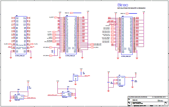
圖24。Bitec DVI HSMC接口板電路圖(1)
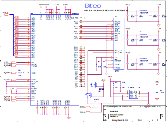
圖25。Bitec DVI HSMC接口板電路圖(2)

圖26。Bitec DVI HSMC接口板電路圖(3)
 電子發(fā)燒友App




評(píng)論