Abstract: Power consumption in battery-backed systems employing microcontrollers is discussed in this application note. Most Dallas Semiconductor high-speed microcontrollers, including the DS87C520, DS89C450, DS80C400 and DS5250 utilize various methods of power management. This application note explores methods of power management such as stop mode, idle mode, optimal clock frequency and external peripherals, to name a few. Sample code is included to highlight new features specifically designed into these microcontrollers to minimize power consumption.
Dallas Semiconductor microcontrollers are manufactured with a Complementary Metal Oxide Semiconductor (CMOS) process that makes them inherently low-power devices. Unlike other technologies, CMOS devices have an infinitesimal quiescent current and only draw significant currents when switching logic states. This means that without further intervention, the user has already designed a low-power system. The power management features of the High-Speed Microcontroller family of microprocessors allow the system designer to effect an even greater reduction in power.
The single largest factor in power consumption of a microcontroller is clock frequency. The power consumed by a microprocessor is directly proportional to its operating speed, so it follows that a device operating at the lowest possible frequency will produce the maximum power savings. The speed chosen depends on the system requirements, most notably interrupt service time. Temperature can also affect power consumption. Semiconductor devices draw greater power at lower temperatures. If the system under development is being designed for cold temperatures, the designer should expect higher than typical power consumption values. System design also has a direct bearing on power consumption, and driving large external loads will increase power consumption.
This application note covers most members of the High-Speed Microcontroller family. Their power management features are explained, and techniques are presented for minimizing power consumption. Because the power management feature operates in conjunction with many of the peripheral functions, especially the interrupt and serial functions, the user is urged to become familiar with the overall operation of the processor before beginning this section.
All the new power-management features were designed to reduce power consumption without sacrificing throughput or responsiveness to external events. Members of this family may contain one or more of these features listed below:
The microcontroller incorporates a ring oscillator to allow for a fast resumption from Stop mode. This provides an instantaneously available 4MHz clock source for the device to start operation. It can function until the crystal has stabilized or can continue to be used as the clock source. The ring oscillator does not exhibit as much stability as an external clock, and the device should not perform timing measurements requiring high accuracy or serial port data transfers while operating from the ring oscillator. For more information concerning the use of the ring oscillator, please consult the Clock Source Control section of this document.
The clock speed management modes are designed to be part of a progressive level of power reduction, based on external activity and performance needs. PMM1 and PMM2 provide the lowest level of power consumption while still permitting full computational and peripheral operation. Figure 1 demonstrates the progression of clock management modes. As explained later, transitions between PMM1 and PMM2 must be made through divide by 4 mode.

Figure 1. Progression of clock speed modes.
Table 1. Clock Divisor Ratet Bit Settings
PMM1 and PMM2 can be exited by configuring the clock divider rate bits CD1, CD0, or by the switchback function. Entry to or exit from either PMM can only be via the divide by 4 mode. For example, to go from PMM1 (divide by 64) to PMM2 (divide by 1024) mode, it is necessary to first switch from PMM1 to divide by 4 mode, and then from divide by 4 to PMM2. Attempts to execute an illegal speed change will be ignored and the bits will remain unchanged. It is the responsibility of the software to test for serial port activity using the Status register (STATUS; C5h) before attempting to change speed. Changing speed during an asynchronous serial port operation will corrupt the serial transmission.
When PMM is invoked, the external crystal will continue to operate at full speed, and the microcontroller will still execute four internal states per machine cycle. In PMM the device performs an internal divide of the external clock, by 16 for PMM1 (16 × 4 = 64) or 256 for PMM2 (256 × 4 = 1024) to achieve the desired frequency, as opposed to actually performing 64 or 256 internal states per instruction. For example, operations that occur during C2 will still do so. Most applications will not find it necessary to attend to this much detail, but the information is provided for calculating critical timings.
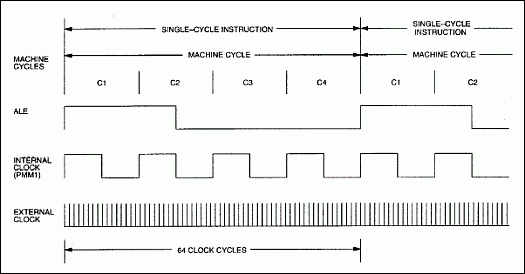
Figure 2. Internal timimg relationships in PMM1.
Note that changing the clock divisor, either manually or through a switchback, will not affect Timed Access procedures. Timed Access operates in relation to internal machine cycles, not an absolute time reference.
Table 2. Effect of Clock Modes on Timer Operation
The watchdog timer runs off the same time base as the internal clocks; i.e., if the device is in PMM1, the watchdog will also be running in a divide by 64 mode. This keeps the watchdog timer synchronized with the operation of the processor when switching between PMM and divide by 4 mode. Applications that use the watchdog timer as an additional timer should take this into account if PMM is used.
The real time clock is independent of the PMM setting. It uses the external 32 kHz crystal as its reference, and can be accessed in any mode.
The benefits of the Status register become apparent when using the switchback feature to exit or enter PMM. A device executing an interrupt service routine in PMM will not execute a switchback in response to an interrupt of equal or lower priority. The Status register can be used to test for an interrupt service routine in progress, and can hold off entering PMM until finished, or take another course of action.
The microcontroller solves this problem by initiating a switchback, if enabled, upon the receipt of a falling edge on the RX pin, not the receiver interrupt. This switches the device back to full speed on the next internal machine cycle in time to capture the start bit and the rest of the transmission. Note that the ability of the serial port to initiate a switchback is not dependent on the Enable Serial Port Interrupt bits (IE.4 or IE.6), only the specific Receiver Enable bit (SCON0.4 or SCON1.4). Four conditions must be met for a serial port reception to cause a switchback:
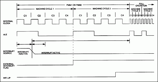
Figure 3. Interrupt-driven switchback.
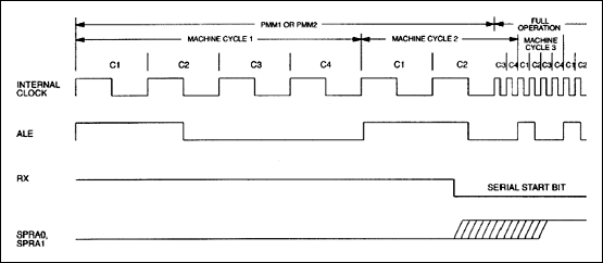
Figure 4. Serial prot driven switchback.
The following example will illustrate how a problem could occur if the priority of the interrupt sources is not taken into account. Assume that the user is employing both Timer 0 and External Interrupt 1 in a design which utilizes PMM. While operating in PMM, a Timer 0 interrupt occurs, and the device begins executing the interrupt service routine (ISR). During the Timer 0 ISR, an External Interrupt 1 occurs, signaling an external event that needs to be serviced quickly. Because both interrupts have the same priority, External Interrupt 1 will remain pending until completion of the Timer 0 ISR. Although such interrupt priorities are a normal consideration in any design, the reduced operating speed in PMM will further increase the latency associated with servicing External Interrupt 1. This could be avoided by specifying External Interrupt 1 as a high priority interrupt and leaving Timer 0 as a low priority interrupt.
A serial port-initiated switchback does not utilize the interrupt structure, and is therefore not affected by interrupt priorities. Serial port-initiated switchbacks are enabled or disabled via the specific receiver enable bit (SCON0.4 or SCON1.4). The ability of a serial port to initiate a switchback is not dependent on the Enable Serial Port Interrupt bits (IE.4 or IE.6).
During a receive operation, the falling edge of the start bit will activate the switchback, if enabled. The serial port activity monitor bit will be set, and the serial port will then check for a valid start bit. If the start bit is received, the serial reception will continue normally, and generate an interrupt when the entire word is received, if enabled. To minimize power consumption, PMM may be enabled again at the start of the serial port interrupt service routine if no further processing is needed in divide by 4 mode.
It is possible to experience a "spurious" switchback caused by a noisy serial port. A switchback is initiated on the first falling edge on the RX pin and begins looking for a valid start bit. If a valid start bit is not received, the system will abort the serial activity, clearing the activity bit, and no serial port interrupt will be executed. The switchback has already been initiated, however, and the device is now operating at full speed. To return the device to PMM, it will be necessary for the user to manually reset the clock rate divider bits.
The code fragment shown in Figure 5 illustrates one possible test for an invalid return to divide by 4 mode. This test can be inserted into the main code loop where it will be periodically executed, or it could be made part of a timer interrupt routine. If no interrupts or serial ports are active, it is likely that the device should be in PMM, not divide by 4 mode. This code should be customized according to the specific configuration, i.e., if a PMM should be allowed in a low priority interrupt, then mask out that bit when testing the Status register.

Figure 5. Invalid switchback test example.
The implication of multiprocessor communications for power management is that a switchback is generated by the detection of the first falling edge on a serial port, not the generation of a valid interrupt. As a result, an invalid address which should be ignored by a particular processor will still generate a switchback. Normally, the part could be returned to PMM at the start of the serial port interrupt service routine. Unfortunately, in the above mentioned case no interrupt will be generated. To alleviate this problem, one should avoid using a multiprocessor communication scheme in conjunction with PMM. If the system power considerations will allow for an occasional erroneous switchback, the polling scheme shown in Figure 5 can be used to place the device back into PMM.
In addition, the ring oscillator eliminates the delay associated with a crystal oscillator and provides an almost instantaneous startup from Stop mode. When used to restart from Stop mode, the ring oscillator will function for a minimum of 65,536 clock cycles, at which time it can automatically switch to the external crystal or continue to run from the ring oscillator. The ring oscillator cannot be used to clock the device from a power-on state, however. Because the ring oscillator does not exhibit as much stability as an external clock, timing measurements or serial port data transfers should not be performed while using the ring oscillator as the clock source.
The ring oscillator finds wide applicability in applications that only require sporadic bursts of processing. Such a system will occasionally awaken from Stop mode, perform some activity, and then return to Stop mode. The ring oscillator allows the system to quickly switch from the lowest power state, perform an operation, and then return to a low power state, without restarting a halted external crystal. Figure 6 shows the advantages of restarting from Stop mode with and without the ring oscillator.
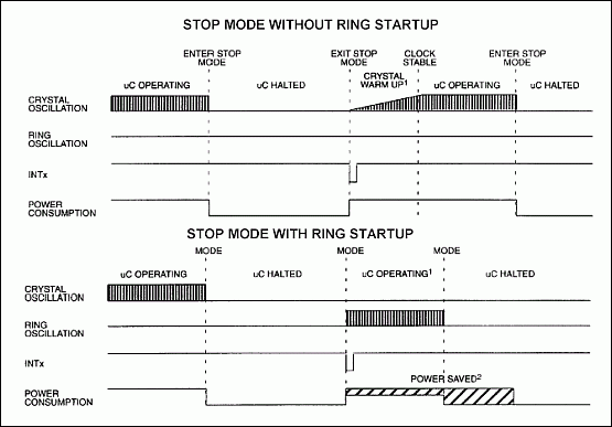
Figure 6. Advantages of ring oscillator.
The status of the crystal startup counter can be determined by reading the Crystal Oscillator Warm-up Status Bit, XTUP (STATUS.4). Note that this bit will always be set upon a power-on reset, because the counter must time out before the device will resume operation. For the same reason, this bit will also be set when resuming from Stop mode with the XT/ "RG-bar" bit set to 1. When switching from the ring oscillator to the crystal oscillator, the XTUP bit can be used to tell when the crystal has stabilized. Attempts to switch to the external crystal before the XTUP bit has been set will be disregarded.
Switching the clock source from the ring oscillator to the crystal oscillator is more involved due to the startup delays inherent in the external crystal. The procedure is as follows:
In the case of external (hardware) and watchdog resets, the XT/ "RG-bar" bit will remain unchanged. This allows the device to continue from the same clock source that was active before the reset event. Regardless of the state of the XT/ "RG-bar" bit, the XTOFF bit is cleared following any reset, which begins the crystal oscillator warm-up. If the crystal will not be used, the appropriate reset routines should set the XTOFF bit to disable the crystal oscillator to conserve power.
Table 4. Clock Source after Stop Mode Determination
If the clock source before entering Stop mode is the ring oscillator, the device will resume operation using the ring oscillator and continue running from the ring oscillator after the crystal warm-up period. If the device enters Stop mode running from the crystal oscillator, the Ring Oscillator Select, Stop Mode bit, RGSL (EXIF.1) determines the clock source when resuming from Stop mode. Upon completion of the crystal warm-up period the device may continue to operate from the ring oscillator, or may switch to the external crystal or clock source. This is determined by the state of the XT/ "RG-bar" bit prior to entering Stop mode.
It should be noted that the crystal amplifier will begin its warm-up period automatically if the XT/ "RG-bar" bit was set prior to entering Stop mode. This will happen if the device was running from the external crystal or external oscillator, or if it was running from the ring oscillator but with the crystal amplifier still running. (Although not a logical choice, this is theoretically possible.) When resuming from the ring oscillator with the intent to continue from the ring oscillator, however, starting the crystal warm-up process is unnecessary. To prevent the crystal warm-up, make sure the device is operating from the ring oscillator and the XTOFF bit is set before entering Stop mode.
The ring oscillator is especially useful for systems which require short bursts of processing upon resuming from Stop mode. Operating from the ring allows the system to wake up, perform a short operation, and return to Stop mode in less time that it would require for an external crystal to stabilize. This provides a two-fold power savings: The time-out of Stop mode is reduced due to the quick start of the ring oscillator, and the ring oscillator itself typically uses less power than the crystal amplifier.
It is not advised to operate the serial ports in asynchronous mode (Modes 1, 2, or 3) while running from the ring oscillator. The serial ports use internal timers to generate their baud rate, and the resulting frequency is not stable enough to support an asynchronous serial transmission. Synchronous serial transmissions in mode 0 are possible, however, due to the synchronizing clock generated by the host processor.
The use of the ring oscillator does not impair the operation of the real time clock, watchdog timer, or timed access operations. The real time clock incorporated in the DS87C530 is excited by an external 32 kHz crystal which is independent of the system clock. The watchdog timer and timed access procedures both function with respect to internal clock cycles, not an absolute time reference, and will operate properly. If an absolute time period is required for the watchdog timer, then an external clock source is recommended.
In the case of a serial transmission, the ring oscillator presents little problem; the system can simply enable the crystal oscillator, wait for the crystal to stabilize, and then begin the transmission. Serial receptions are more difficult. There is no way that a microcontroller operating from a ring oscillator will be able to successfully capture a serial data transfer on the first try. One possible solution would be to employ a handshaking protocol to confirm that the receiver is ready and the data should be resent. The key in such a scheme is to detect that a serial operation has been attempted and execute a section of code that will switch over to the crystal source.
The recommended approach utilizes an external interrupt as a serial port activity monitor. If a negative edge triggered interrupt such as /INTO\ , /INT1\ , /INT3\ , or /INT5\ is tied to the RX pin, the falling edge of a start bit will generate an interrupt and a switchback. The interrupt service routine will enable the crystal clock source and wait until it is stable, at which time the device will transmit a ready signal back to the originator. The following code example demonstrates one way to do this.
In addition, the delay associated with restarting the crystal can be avoided by keeping the crystal amplifier enabled when running from the ring oscillator. This seems counterproductive at first, as it increases the power consumption slightly when compared to running from the ring oscillator alone. However, when operating the device from a relatively high-speed crystal, the reduced speed of the ring oscillator still results in a net power savings.
The determination of which power management modes to utilize, when to switch modes, and how to handle high-priority tasks is application-dependent. No single approach will suit all possible combinations. In general, the selection of clock speeds and sources depends on the assigned tasks, and the need for timing-dependent operations such as serial ports activity.
There are two basic classes of systems which employ power management. The first is systems which hibernate or spend almost all of their operating time in a standby state, such as Stop or PMM2. These systems are often used in unattended systems to gather data or as environmental monitors. They are characterized by relatively infrequent I/O activity at specific intervals. The second class of systems usually performs a high rate of I/O activity on several devices, or otherwise must be operating constantly. A hibernation approach would be impractical in this instance as the device would spend most of its time simply restarting from the low-power state. These two approaches are discussed in more detail in the following sections.
The decision on what to designate as the standby state depends on the type of activity that will initiate a return to the active state. If serial port activity is expected, then the standby state must be one that can receive serial data, such as PMM2. A system which can tolerate longer interrupt latencies can use Stop mode as the low power state.
An examination of the power consumption in the various modes shows that when using a burst-mode approach, the most power savings can be gained by operating in divide by 4 mode, rather than the PMMs. Divide by 4 mode gives 16 times the performance of PMM1, but consumes only four times the current. The higher power/performance ratio of divide by 4 mode means that less total energy will be consumed during the subroutine. As a result, routines that wake from Stop mode to perform short bursts of activity and then return to Stop should do so in divide by 4 mode.
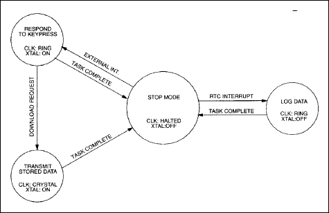
Figure 7. Remote data logger example state diagram.
The decision of when to switch modes and which modes to switch between is dependent on the user's application. Constructing a "power path" is the simplest way to determine what speeds and clock source are appropriate. For a relatively simple system, only a few states are needed. The power management modes PMM1 and PMM2 were specifically designed to be part of such a gradual power reduction.
Figure 8 demonstrates a number of power paths possible with the power management capabilities. Figure 8a shows a relatively complicated scheme which performs a gradual reduction in operating speed, while keeping the clock oscillator operating as long as possible to perform timing-dependent functions. Figure 8b switches to the ring oscillator and gradually reduces the speed of the device, but keeps the crystal amplifier enabled in case the device needs to quickly respond to serial port activity. Figure 8c provides the lowest power consumption by switching to the ring oscillator and disabling the crystal amplifier.
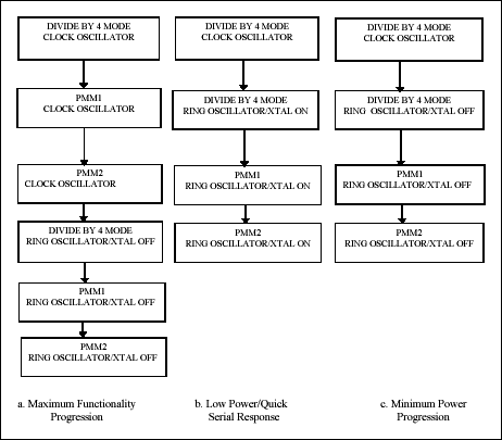
Figure 8. Sample power paths.
The program monitors a peripheral on port 1 and updates a display mapped into external memory as needed. The watchdog timer is used to poll the status of the system, which is indicated by the F0 flag. If there is no activity before the timer times out, the device will continue to decrease its speed. Because the watchdog timer period is affected by the speed of the device, the watchdog divide ratio is adjusted to keep as constant an interval as possible. The methods demonstrated could also be used to detect a spurious switchback caused by noise on the serial port and return the device to PMM.
Setting the Bandgap Select bit, BGS (EXIF.0) enables the bandgap reference during Stop mode. The default or reset condition is with the bit cleared, and the bandgap disabled during Stop mode. Note that this bit can be only changed using a timed access write. It has no control of the reference during full power, PMM, or Idle modes.
Overview
Power management is critical in battery-powered applications. Differences of microamperes can translate into months or years of operating life, which can make or break a product in the marketplace. The high level of integration of Dallas Semiconductor microcontrollers makes them ideal for portable or battery-operated applications that demand low power consumption. By combining the processor and peripherals onto a single die, redundant hardware is eliminated, and power savings are achieved. In addition, power management features designed into the High-Speed Microcontroller family further reduce power consumption.Dallas Semiconductor microcontrollers are manufactured with a Complementary Metal Oxide Semiconductor (CMOS) process that makes them inherently low-power devices. Unlike other technologies, CMOS devices have an infinitesimal quiescent current and only draw significant currents when switching logic states. This means that without further intervention, the user has already designed a low-power system. The power management features of the High-Speed Microcontroller family of microprocessors allow the system designer to effect an even greater reduction in power.
The single largest factor in power consumption of a microcontroller is clock frequency. The power consumed by a microprocessor is directly proportional to its operating speed, so it follows that a device operating at the lowest possible frequency will produce the maximum power savings. The speed chosen depends on the system requirements, most notably interrupt service time. Temperature can also affect power consumption. Semiconductor devices draw greater power at lower temperatures. If the system under development is being designed for cold temperatures, the designer should expect higher than typical power consumption values. System design also has a direct bearing on power consumption, and driving large external loads will increase power consumption.
This application note covers most members of the High-Speed Microcontroller family. Their power management features are explained, and techniques are presented for minimizing power consumption. Because the power management feature operates in conjunction with many of the peripheral functions, especially the interrupt and serial functions, the user is urged to become familiar with the overall operation of the processor before beginning this section.
All the new power-management features were designed to reduce power consumption without sacrificing throughput or responsiveness to external events. Members of this family may contain one or more of these features listed below:
Dynamic Clock Speed Control
The High-Speed Microcontrollers support four clock management modes: Stop, PMM1 (Power Management Mode 1), PMM2 (Power Management Mode 2), and Idle. They can dynamically switch between these modes, allowing the user to optimize the speed of the device while minimizing power consumption. The Stop mode has been improved over standard 8051 capabilities, and now supports resume from external interrupts as well as reset sources.Switchback
The devices incorporate an automatic "switchback" feature to allow a device operating in a Power Management Mode (PMM) to switch into "high gear" upon receipt of an external interrupt or serial port transmission. This enables a device in power-saving mode to respond quickly to external events and/or operate its serial ports. Traditional 8051-based devices without the switchback feature lose the ability to service interrupts quickly without running the device at high speed, and higher power consumption, constantly.Selectable Clock Source
The crystal oscillator is a large consumer of power on any microcontroller, especially during low power operation. The ring oscillator, used for quick starts from Stop mode, can also be used to provide an approximately 3 to 4MHz clock source during normal operation. Although a crystal oscillator is still required at power-up, once the crystal has stabilized, device operation can be switched to the ring oscillator, realizing a power savings of as much as 25 mA.Bandgap Reference Disabling
The option is available to disable the bandgap reference, which is used to detect a power failure while in Stop mode. Stop mode current can be greatly using this feature.Enhanced Status Reporting
Although the ability to dynamically switch the internal clock speed is a benefit, if performed at the wrong time it can seriously interfere with the operation of timing-dependent functions. The Status register (STATUS;C5h), contains information about the status of both serial ports, the crystal oscillator, and high priority, low priority, and power-fail interrupts. The software can delay or cancel a planned speed change based on the information in this register.Clock Speed Control
Description
The operating frequency of a microcontroller is the single biggest factor in determining power consumption. The High-Speed Microcontroller family of microcontrollers supports four clock speed management modes that conserve power by slowing or stopping the internal clock. These modes allow the system designer to maximize power savings with a minimum impact on performance.PMM1
Power Management Mode 1 (PMM1) allows the user to run at a reduced speed to save power. Setting the clock divider rate bits (PMR.7-6) will force the part from its default 4 clocks per machine cycle (divide by 4) to 64 clocks per machine cycle (divide by 64). The external crystal continues to operate at full speed. All peripherals and instructions will operate at this reduced speed. The microcontroller can resume divide by 4 operation by setting the appropriate clock divider rate bits or by utilizing the switchback feature.PMM2
Power Management Mode 2 (PMM2) allows the user to run at an even slower speed to improve power savings. Setting the clock divider rate bits (PMR.7-6) will force the part from its default 4 clocks per machine cycle (divide by 4) to 1024 clocks per machine cycle (divide by 1024). The external crystal continues to operate at full speed. All peripherals and instructions will operate at this reduced speed. The microcontroller can resume full-speed (divide by 4) operation by setting the appropriate clock divider rate bits or by utilizing the switchback feature. This mode permits an even greater power savings over PMM1.Stop Mode
The Stop mode is the lowest power state available. It is initiated by setting the Stop bit (PCON.1). While in this mode the crystal oscillator is stopped, and all internal clocking, including the Watchdog Timer, is halted. The real time clock is unaffected by Stop mode. The Stop mode is exited by an external interrupt, real-time clock interrupt, an external reset via the RST pin, or a power-on reset. Each interrupt will cause the device to vector to the corresponding interrupt routine to resume execution.The microcontroller incorporates a ring oscillator to allow for a fast resumption from Stop mode. This provides an instantaneously available 4MHz clock source for the device to start operation. It can function until the crystal has stabilized or can continue to be used as the clock source. The ring oscillator does not exhibit as much stability as an external clock, and the device should not perform timing measurements requiring high accuracy or serial port data transfers while operating from the ring oscillator. For more information concerning the use of the ring oscillator, please consult the Clock Source Control section of this document.
Idle Mode
The Idle mode halts operation of the microcontroller processor core but leaves internal clocks, serial ports, and timers running. This mode is invoked by setting the IDL bit (PCON.0) and can be exited by an interrupt or external reset via the RST pin. Use of this mode is not recommended on new designs, as lower power operation can be achieved by placing the part in PMM2 and executing NOPs. Its inclusion provides backward software compatibility.Power Management Modes
The greatest power savings come from utilizing the power management modes. Unlike other techniques, Power Management Modes 1 and 2 (PMM1 and PMM2) allow the user to reduce power consumption without sacrificing performance. Although the power management features are an important part of a power efficient design, a thorough understanding of the microprocessor will allow the system designer to achieve maximum power savings.The clock speed management modes are designed to be part of a progressive level of power reduction, based on external activity and performance needs. PMM1 and PMM2 provide the lowest level of power consumption while still permitting full computational and peripheral operation. Figure 1 demonstrates the progression of clock management modes. As explained later, transitions between PMM1 and PMM2 must be made through divide by 4 mode.

Figure 1. Progression of clock speed modes.
Entering and Exiting Power Management Modes
Software invokes the desired power management mode using bits in the Power Management Register (PMR). Stop mode is invoked by setting the STOP bit (PCON.1). The device speed is selected by the clock divider rate bits CD1, CD0 (PMR.7-6), shown below.Table 1. Clock Divisor Ratet Bit Settings
| CD1 | CD0 | MACHINE CYCLE RATE |
| 0 | 0 | Reserved |
| 0 | 1 | 4 clocks (default) |
| 1 | 0 | 64 clocks (PMM1) |
| 1 | 1 | 1024 clocks (PMM2) |
PMM1 and PMM2 can be exited by configuring the clock divider rate bits CD1, CD0, or by the switchback function. Entry to or exit from either PMM can only be via the divide by 4 mode. For example, to go from PMM1 (divide by 64) to PMM2 (divide by 1024) mode, it is necessary to first switch from PMM1 to divide by 4 mode, and then from divide by 4 to PMM2. Attempts to execute an illegal speed change will be ignored and the bits will remain unchanged. It is the responsibility of the software to test for serial port activity using the Status register (STATUS; C5h) before attempting to change speed. Changing speed during an asynchronous serial port operation will corrupt the serial transmission.
When PMM is invoked, the external crystal will continue to operate at full speed, and the microcontroller will still execute four internal states per machine cycle. In PMM the device performs an internal divide of the external clock, by 16 for PMM1 (16 × 4 = 64) or 256 for PMM2 (256 × 4 = 1024) to achieve the desired frequency, as opposed to actually performing 64 or 256 internal states per instruction. For example, operations that occur during C2 will still do so. Most applications will not find it necessary to attend to this much detail, but the information is provided for calculating critical timings.

Figure 2. Internal timimg relationships in PMM1.
Note that changing the clock divisor, either manually or through a switchback, will not affect Timed Access procedures. Timed Access operates in relation to internal machine cycles, not an absolute time reference.
Timers and PMM
Timers 0, 1, and 2 will default on power-up to a 12 external clocks per timer tick to remain compatible with the original 8051/8032 specifications. The timers can be individually configured to run at a rate of four external clocks per timer tick when the device is operating in divide by 4 mode by setting the relevant bits in the Clock Control Register (CKCON;8Eh). During PMM timers 0, 1, and 2 operate at correspondingly reduced clock rates, because the timers derive their time base from the internal clock. This will also affect the operation of the serial ports in PMM as theTable 2. Effect of Clock Modes on Timer Operation
| CD1 | CD0 | OSC. CYCLES PER MACHINE CYCLE | OSC CYCLES PER TIMER 0/1/2 CLOCK | OSC CYCLES PER TIMER 2 CLOCK, BAUD RATE GEN. | OSC CYCLES PER SERIAL PORT CLOCK MODE 0 | OSC. CYCLES PER SERIAL PORT CLOCK MODE 2 | ||||
| TxM=1 | TxM=0 | T2M=1 | T2M=0 | SM2=0 | SM2=1 | SMOD=0 | SMOD=1 | |||
| 0 | 0 | Reserved | ? | ? | ? | ? | ? | ? | ? | ? |
| 0 | 1 | 4 | 12 | 4 | 2 | 2 | 12 | 4 | 64 | 32 |
| 1 | 0 | 64(PMM1) | 192 | 64 | 32 | 32 | 192 | 64 | 1024 | 512 |
| 1 | 1 | 1024 (PMM2) | 3072 | 1024 | 512 | 512 | 3072 | 1024 | 16,384 | 8192 |
The watchdog timer runs off the same time base as the internal clocks; i.e., if the device is in PMM1, the watchdog will also be running in a divide by 64 mode. This keeps the watchdog timer synchronized with the operation of the processor when switching between PMM and divide by 4 mode. Applications that use the watchdog timer as an additional timer should take this into account if PMM is used.
The real time clock is independent of the PMM setting. It uses the external 32 kHz crystal as its reference, and can be accessed in any mode.
Manually Exiting PMM
In addition to the switchback feature, it is also possible to manually exit a PMM by configuring the clock divider rate bits. Entry to or exit from either PMM can only be via the divide by 4 mode, and attempts to execute an illegal speed change will be ignored and the bits will remain unchanged. If a timing-dependent operation may be in progress, the Status register (STATUS;C5h) should be interrogated to determine if it has been completed before switching out of or into PMM.Reset Sensitivity in PMM
While in PMM, the method used to detect an external reset pulse differs from that used in divide by 4 mode. In divide by 4 mode, (and standard 8051 architecture) a reset must be high for two machine cycles to be detected. If this were true in PMM, reset would have to be asserted for a minimum of 128 or 2048 clock cycles. To avoid this, devices operating in PMM employ a positive edge-detect sensor, rather than a one machine cycle qualification to detect a reset signal. This means that devices which use PMM are more susceptible to noise and additional care must be taken to keep the reset signal noise-free.Switchback Feature
The switchback feature allows the user to quickly restore the microcontroller to a higher speed when an event occurs. When enabled, a qualified event causes the device to automatically switch from divide by 64 (PMM1) or divide by 1024 (PMM2) to divide by 4 operation without software intervention. This allows the device to respond to high priority or interrupt driven events with a minimum delay. The following sources can trigger a switchback:- external interrupt 0/1/2/3/4/5
- serial start bit detected, Serial Port 0/1
- transmit buffer loaded, Serial Port 0/1
- watchdog timer reset
- power-on reset
- external reset
Status Register
A Status register (STATUS;C5h) has been added to aid the software in determining whether a speed change is appropriate. The Status register provides information on the status of both serial ports, and high priority, low priority, and power-fail interrupts, allowing the device to determine whether or not the device should be switched into PMM.The benefits of the Status register become apparent when using the switchback feature to exit or enter PMM. A device executing an interrupt service routine in PMM will not execute a switchback in response to an interrupt of equal or lower priority. The Status register can be used to test for an interrupt service routine in progress, and can hold off entering PMM until finished, or take another course of action.
Enabling/Initiating Switchback
Automatic switchback is enabled by setting the SWB bit (PMR.5). When a qualified switchback event occurs, the device will exit either PMM and return to the default operating mode of 4 clocks per machine cycle. Clearing the SWB bit will disable the ability of external interrupts and serial ports to cause future switchbacks, but will not affect the current speed. Five conditions must be met for an external interrupt to cause a switchback:- The device must currently be in PMM1 or PMM2.
- The SWB bit (PMR.5) must be set.
- Global interrupts must be enabled by setting the EA bit (IE.7).
- The specific interrupt must be enabled.
- The specific interrupt occurs and is acknowledged.
The microcontroller solves this problem by initiating a switchback, if enabled, upon the receipt of a falling edge on the RX pin, not the receiver interrupt. This switches the device back to full speed on the next internal machine cycle in time to capture the start bit and the rest of the transmission. Note that the ability of the serial port to initiate a switchback is not dependent on the Enable Serial Port Interrupt bits (IE.4 or IE.6), only the specific Receiver Enable bit (SCON0.4 or SCON1.4). Four conditions must be met for a serial port reception to cause a switchback:
- The device must currently be in PMM1 or PMM2.
- The SWB bit (PMR.5) must be set.
- The specific serial port must be enabled by setting the specific Receiver Enable bit (SCON0.4 or
- SCON1.4).
- A falling edge is detected on the specific RX pin.
- The device must currently be in PMM1 or PMM2.
- The SWB bit (PMR.5) must be set.
- A serial port transmission must be initiated by loading the specific serial port buffer (SBUF0;99h or SBUF1;C1h).
Considerations When Using Switchback
Switchback Timing
One of the primary considerations when using the switchback procedure is the time required to return the device to full speed from a PMM. This is a factor in calculating the latency associated with servicing an interrupt. Switchbacks will occur at the C1 cycle of the first instruction following the event initiating the switchback. If the current instruction in progress is a write to the IE, IP, EIP or EIE register, interrupt processing will be delayed until the completion of the following instruction. Figure 3 demonstrates the timing relationship between interrupts and switchbacks during a two-cycle instruction.
Figure 3. Interrupt-driven switchback.
NOTES:
- Internal clock cycle is 16 external clock cycles for PMM1 and 256 external clock cycles for PMM2.
- Polarity of interrupt varies with respect to external interrupt number.
- Example shows two-cycle instruction. Execution of the interrupt and switchback will occur at the end of the last machine cycle of the instruction in which the interrupt is acknowledged.

Figure 4. Serial prot driven switchback.
NOTES:
- Internal Cx cycle is 16 external clock cycles for PMM1 and 256 external clock cycles for PMM2.
- SPRA0 and SPRA1 will change within 1 machine cycle of the falling edge RX.
- Example shows single-cycle instructions. Execution of the interrupt and switchback will occur at the end of the last machine cycle of the instruction in which the interrupt is acknowledged.
Interrupt Priority
Because the switchback feature uses interrupts to qualify execution, it is affected by interrupt priorities. The external interrupts initiate a switchback upon the start of the interrupt service routine. If a higher priority interrupt is in progress, the associated switchback will remain pending. It is not possible to enable or disable the switchback function for individual interrupt sources, except by enabling or disabling the specific interrupt.The following example will illustrate how a problem could occur if the priority of the interrupt sources is not taken into account. Assume that the user is employing both Timer 0 and External Interrupt 1 in a design which utilizes PMM. While operating in PMM, a Timer 0 interrupt occurs, and the device begins executing the interrupt service routine (ISR). During the Timer 0 ISR, an External Interrupt 1 occurs, signaling an external event that needs to be serviced quickly. Because both interrupts have the same priority, External Interrupt 1 will remain pending until completion of the Timer 0 ISR. Although such interrupt priorities are a normal consideration in any design, the reduced operating speed in PMM will further increase the latency associated with servicing External Interrupt 1. This could be avoided by specifying External Interrupt 1 as a high priority interrupt and leaving Timer 0 as a low priority interrupt.
A serial port-initiated switchback does not utilize the interrupt structure, and is therefore not affected by interrupt priorities. Serial port-initiated switchbacks are enabled or disabled via the specific receiver enable bit (SCON0.4 or SCON1.4). The ability of a serial port to initiate a switchback is not dependent on the Enable Serial Port Interrupt bits (IE.4 or IE.6).
Serial Port Activity and PMM
Because the function of PMM is to change the internal clock frequency of the microcontroller, timing-dependent peripherals such as the serial ports can be affected. The user must be sure that the serial ports are not receiving or transmitting when switching into PMM. The simplest way to do this is to interrogate the serial port activity bits in the Status register (STATUS.3-0).During a receive operation, the falling edge of the start bit will activate the switchback, if enabled. The serial port activity monitor bit will be set, and the serial port will then check for a valid start bit. If the start bit is received, the serial reception will continue normally, and generate an interrupt when the entire word is received, if enabled. To minimize power consumption, PMM may be enabled again at the start of the serial port interrupt service routine if no further processing is needed in divide by 4 mode.
It is possible to experience a "spurious" switchback caused by a noisy serial port. A switchback is initiated on the first falling edge on the RX pin and begins looking for a valid start bit. If a valid start bit is not received, the system will abort the serial activity, clearing the activity bit, and no serial port interrupt will be executed. The switchback has already been initiated, however, and the device is now operating at full speed. To return the device to PMM, it will be necessary for the user to manually reset the clock rate divider bits.
The code fragment shown in Figure 5 illustrates one possible test for an invalid return to divide by 4 mode. This test can be inserted into the main code loop where it will be periodically executed, or it could be made part of a timer interrupt routine. If no interrupts or serial ports are active, it is likely that the device should be in PMM, not divide by 4 mode. This code should be customized according to the specific configuration, i.e., if a PMM should be allowed in a low priority interrupt, then mask out that bit when testing the Status register.

Figure 5. Invalid switchback test example.
Multiprocessor Communications in PMM
The effectiveness of PMM and the switchback feature is affected if multiprocessor communications protocols are used. The microcontroller includes features that will support multiple processors on the same serial port. In serial port modes 2 and 3 it is possible to use the SM2 flag (SCON0.5 or SCON1.5) to signify that the received byte is an address. The slave address recognition registers (SADDR0;A9h, SADDR1;AAh, SADEN0;B9h, SADEN1;BAh) can be programmed to ignore a transmission (not cause a receiver interrupt) when a received address does not match a user-defined pattern.The implication of multiprocessor communications for power management is that a switchback is generated by the detection of the first falling edge on a serial port, not the generation of a valid interrupt. As a result, an invalid address which should be ignored by a particular processor will still generate a switchback. Normally, the part could be returned to PMM at the start of the serial port interrupt service routine. Unfortunately, in the above mentioned case no interrupt will be generated. To alleviate this problem, one should avoid using a multiprocessor communication scheme in conjunction with PMM. If the system power considerations will allow for an occasional erroneous switchback, the polling scheme shown in Figure 5 can be used to place the device back into PMM.
Clock Source Control
By controlling the source of the system clock, the system designer can simultaneously achieve higher performance and decreased power consumption. To provide maximum flexibility, the microcontroller will operate from three clock sources:- External Crystal (using internal crystal oscillator)
- External Clock Oscillator
- Internal Ring Oscillator
External Crystal
The most common clocking source is an external crystal. The microcontroller incorporates a crystal amplifier which is designed to drive industry standard crystals over the operating range of the device. External crystals provide a highly accurate clock source for timing-dependent peripherals such as internal timers and serial ports, as well as device operation. The microcontroller requires a fundamental-mode, parallel-resonant (also called anti-resonant) AT-cut crystal. Crystal oscillators have significant start-up times, however, which can delay the operation of the device when powering on or resuming from the Stop mode. The microcontroller must start operation with an external crystal or external clock source after a power-on reset.External Clock Source
If a clock oscillator is already present in the system, it can be used as the external clock source. External clock oscillators suffer from the same start-up delays as the internal crystal oscillator and do not provide any special benefits. Either an external crystal or external clock source can be used to clock the device following a power-on reset or power-fail reset.Ring Oscillator
The ring oscillator is a low-power digital oscillator internal to the microcontroller. It can be used as the primary system clock, instead of an external crystal or clock oscillator, at any time except immediately following a power-on reset. When enabled, it provides a 4MHz clock source for device operation. This is typically a lower frequency than the system clock, and this provides a significant power savings. Once the device has switched to the ring oscillator as the clock source, the external crystal amplifier can be disabled, further reducing power consumption.In addition, the ring oscillator eliminates the delay associated with a crystal oscillator and provides an almost instantaneous startup from Stop mode. When used to restart from Stop mode, the ring oscillator will function for a minimum of 65,536 clock cycles, at which time it can automatically switch to the external crystal or continue to run from the ring oscillator. The ring oscillator cannot be used to clock the device from a power-on state, however. Because the ring oscillator does not exhibit as much stability as an external clock, timing measurements or serial port data transfers should not be performed while using the ring oscillator as the clock source.
The ring oscillator finds wide applicability in applications that only require sporadic bursts of processing. Such a system will occasionally awaken from Stop mode, perform some activity, and then return to Stop mode. The ring oscillator allows the system to quickly switch from the lowest power state, perform an operation, and then return to a low power state, without restarting a halted external crystal. Figure 6 shows the advantages of restarting from Stop mode with and without the ring oscillator.

Figure 6. Advantages of ring oscillator.
- Diagram assumes that the operation following Stop requires less than 18 ms to complete.
- Additional power savings due to decreased ring oscillation current compared to crystal amplifier.
Clock Control Bits
Table 3. Clock Control and Status Bit Summary| BIT NAME | LOCATION | FUNCTION | RESET | WRITE ACCESS |
| XT/ "RG-bar" | EXIF.3 | Crystal/Ring Clock Source Select 0= Select ring oscillator as clock source 1= Select crystal or external clock as clock source. |
1 | 0 anytime; 1 when XTUP= 1 and XTOFF= 0 |
| RGMD | EXIF.2 | Ring Oscillator Mode Status. 0= Crystal or external clock is current clock source. 1= Ring oscillator is current clock source. |
0 | None |
| RGSL | EXIF.1 | Ring Oscillator Select, Stop Mode. 0= Crystal or external clock will be the clock source when resuming Stop mode. 1= Ring oscillator will be the clock source when resuming from Stop mode Note: Upon completion of crystal warm up period, device will switch to clock source designated by XT/ "RG-bar" bit. |
Unchanged except after power-on reset, when it is cleared to 0. |
Unrestricted |
| XTOFF | PMR.3 | Crystal Oscillator Disable. 0= Crystal oscillator is enabled. 1= Crystal oscillator is disabled. Device is operating from ring oscillator. |
0 | 0 anytime; 1 when XT/ "RG-bar"= 0 |
| XTUP | STATUS.4 | Crystal Oscillator Warm-up Status. 0= Oscillator warm-up still in progress. 1= Oscillator warm-up complete. |
1 | None |
Crystal Oscillator Startup Delay
When power is applied to a crystal oscillator after a period of non-operation, a short period of time is required before the amplitude of the pulse is sufficient to provide a stable clock source. This can result in missed or corrupted clock signals, possibly disrupting processor operation. To ensure a valid clock signal, a crystal startup counter detects 65,536 oscillations of the external crystal or clock oscillator before allowing the device to resume operation. This means that devices utilizing slower crystals will have longer crystal startup times. The crystal startup counter is more sensitive than the internal clock circuitry, and uses the count of both bad and good pulses determine the warm-up period. The counter value was chosen to allow the majority of crystals enough time to stabilize before releasing the device to run off the external crystal. The counter is reset anytime the XTOFF bit is cleared.The status of the crystal startup counter can be determined by reading the Crystal Oscillator Warm-up Status Bit, XTUP (STATUS.4). Note that this bit will always be set upon a power-on reset, because the counter must time out before the device will resume operation. For the same reason, this bit will also be set when resuming from Stop mode with the XT/ "RG-bar" bit set to 1. When switching from the ring oscillator to the crystal oscillator, the XTUP bit can be used to tell when the crystal has stabilized. Attempts to switch to the external crystal before the XTUP bit has been set will be disregarded.
Switching Between Clock Sources
On occasion the device may wish to switch between the ring oscillator and crystal oscillator. The device can switch to the ring oscillator at any time as there is no start-up delay associated with the ring oscillator. Clearing the Crystal Oscillator/Ring Oscillator Select Bit, XT/ "RG-bar" (EXIF.3) will enable the ring oscillator. If there is no expectation that the crystal oscillator will be needed soon, the crystal oscillator can be disabled by setting the Crystal Oscillator Disable Bit, XTOFF (PMR.3). This will provide a significant power savings. Note that clearing the XT/ "RG-bar" bit does not automatically disable the crystal amplifier.Switching the clock source from the ring oscillator to the crystal oscillator is more involved due to the startup delays inherent in the external crystal. The procedure is as follows:
- Clear the Crystal Oscillator Disable Bit, XTOFF (PMR.3) to restart the crystal oscillator.
- Wait for the Crystal Oscillator Warm-up Status bit, XTUP (STATUS.4) to be set, indicating that the external crystal warm up period is complete.
- Set the Crystal Oscillator/Ring Oscillator Select Bit, XT/RG (EXIF.3) to select the crystal as the clock source.
Clock Source After Reset
Following a power-on reset, the RGSL bit is cleared and the XT/ "RG-bar" bit is set. This forces the device to operate from an external crystal or external clock source, regardless of the clock source prior to the event. The crystal start-up counter will be reset and begin counting down, allowing time for the crystal to stabilize before resuming operation.In the case of external (hardware) and watchdog resets, the XT/ "RG-bar" bit will remain unchanged. This allows the device to continue from the same clock source that was active before the reset event. Regardless of the state of the XT/ "RG-bar" bit, the XTOFF bit is cleared following any reset, which begins the crystal oscillator warm-up. If the crystal will not be used, the appropriate reset routines should set the XTOFF bit to disable the crystal oscillator to conserve power.
Clock Source After Stop
During Stop mode internal clocking is halted. Upon receipt of an external interrupt or reset the device will use the state of the XTOFF, XT/ "RG-bar", and RGSL bits prior to entering Stop mode to determine the state of the ring oscillator and crystal amplifier. The possible configurations are shown in Table 4.Table 4. Clock Source after Stop Mode Determination
| XT/ "RG-bar" | XTOFF | RGSL | CLOCK SOURCE WHEN EXITING STOP MODE | CLOCK SOURCE AFTER CRYSTAL WARM-UP PERIOD | STARTUP DELAY WHEN RESUMING? | CRYSTAL OSCILLATOR STATUS |
| 0 | 0 | x | Ring Oscillator | Ring Oscillator | No | Enabled |
| 0 | 1 | x | Ring Oscillator | Ring Oscillator | No | Disabled |
| 1 | 0 | 0 | Crystal Oscillator | Crystal Oscillator | Yes | Enabled |
| 1 | 0 | 1 | Ring Oscillator | Crystal Oscillator | No | Enabled |
If the clock source before entering Stop mode is the ring oscillator, the device will resume operation using the ring oscillator and continue running from the ring oscillator after the crystal warm-up period. If the device enters Stop mode running from the crystal oscillator, the Ring Oscillator Select, Stop Mode bit, RGSL (EXIF.1) determines the clock source when resuming from Stop mode. Upon completion of the crystal warm-up period the device may continue to operate from the ring oscillator, or may switch to the external crystal or clock source. This is determined by the state of the XT/ "RG-bar" bit prior to entering Stop mode.
It should be noted that the crystal amplifier will begin its warm-up period automatically if the XT/ "RG-bar" bit was set prior to entering Stop mode. This will happen if the device was running from the external crystal or external oscillator, or if it was running from the ring oscillator but with the crystal amplifier still running. (Although not a logical choice, this is theoretically possible.) When resuming from the ring oscillator with the intent to continue from the ring oscillator, however, starting the crystal warm-up process is unnecessary. To prevent the crystal warm-up, make sure the device is operating from the ring oscillator and the XTOFF bit is set before entering Stop mode.
The ring oscillator is especially useful for systems which require short bursts of processing upon resuming from Stop mode. Operating from the ring allows the system to wake up, perform a short operation, and return to Stop mode in less time that it would require for an external crystal to stabilize. This provides a two-fold power savings: The time-out of Stop mode is reduced due to the quick start of the ring oscillator, and the ring oscillator itself typically uses less power than the crystal amplifier.
Ring Oscillator Considerations
The ring oscillator used in the High-Speed Microcontroller Family is essentially a chain of inverters with a propagation delay. Although it exhibits fast start-up times, it does not carry the stability of a piezoelectric quartz crystal oscillator. The ring oscillator will oscillate from 3 to 4MHz over the temperature and voltage range specified for the device. This variation makes it difficult to generate a stable time base for timers and timing-sensitive operations. Interrupt latencies will also be more difficult to calculate due to the variation of the main system clock.It is not advised to operate the serial ports in asynchronous mode (Modes 1, 2, or 3) while running from the ring oscillator. The serial ports use internal timers to generate their baud rate, and the resulting frequency is not stable enough to support an asynchronous serial transmission. Synchronous serial transmissions in mode 0 are possible, however, due to the synchronizing clock generated by the host processor.
The use of the ring oscillator does not impair the operation of the real time clock, watchdog timer, or timed access operations. The real time clock incorporated in the DS87C530 is excited by an external 32 kHz crystal which is independent of the system clock. The watchdog timer and timed access procedures both function with respect to internal clock cycles, not an absolute time reference, and will operate properly. If an absolute time period is required for the watchdog timer, then an external clock source is recommended.
Performing a "Ring-Oscillator Switchback"
The switchback feature allows the device to "wake up" for serial port operations when operating in PMM1 or PMM2. Although the device will execute a switchback regardless of the clock source, the device must be operating from a crystal or external clock source for the serial operation to be successful. In most cases, this would preclude the use of the ring oscillator or Stop mode if serial port operations are expected. However, it is possible to "switchback" from the ring oscillator to the crystal upon receipt of a serial transmission.In the case of a serial transmission, the ring oscillator presents little problem; the system can simply enable the crystal oscillator, wait for the crystal to stabilize, and then begin the transmission. Serial receptions are more difficult. There is no way that a microcontroller operating from a ring oscillator will be able to successfully capture a serial data transfer on the first try. One possible solution would be to employ a handshaking protocol to confirm that the receiver is ready and the data should be resent. The key in such a scheme is to detect that a serial operation has been attempted and execute a section of code that will switch over to the crystal source.
The recommended approach utilizes an external interrupt as a serial port activity monitor. If a negative edge triggered interrupt such as /INTO\ , /INT1\ , /INT3\ , or /INT5\ is tied to the RX pin, the falling edge of a start bit will generate an interrupt and a switchback. The interrupt service routine will enable the crystal clock source and wait until it is stable, at which time the device will transmit a ready signal back to the originator. The following code example demonstrates one way to do this.
In addition, the delay associated with restarting the crystal can be avoided by keeping the crystal amplifier enabled when running from the ring oscillator. This seems counterproductive at first, as it increases the power consumption slightly when compared to running from the ring oscillator alone. However, when operating the device from a relatively high-speed crystal, the reduced speed of the ring oscillator still results in a net power savings.
Program Example: Software Ring Oscillator Switchback
;Program RING_SWB
;
;This program shows how the serial ports can be operated in conjunction with
;the ring oscillator. When receiving a byte, the falling edge of the start
;bit will generate an INT1. The INT1 ISR will restart the crystal oscillator.
;When the crystal has stabilized, the system will transmit a ready character
;to the originator to indicate that the receiver is ready.
;
;The core of the program continuously scans Port 1 and records the maximum
;value. The program performs two operations: transmit the maximum
;recorded value, and reset the maximum value to 0. Receipt of an invalid
;command will cause the device to return an error code to the host and
;switch back to the ring oscillator. Invalid codes can also be used to
;intentionally return the device to the ring oscillator at the completion
;of the data transfer. Valid commands will be echoed back to the originator
;to confirm receipt.
;***************************************************************************
;Register Equates
P0 equ 80h ;Port 0
SP equ 81h ;Stack Pointer
PCON equ 87h ;Power Control Register
TMOD equ 89h ;Timer Mode Control Register
TH1 equ 8Dh ;Timer 1 MSB (used for baud rate generation)
P1 equ 90h ;Port 1
EXIF equ 91h ;External Interrupt Flag Register
SCON0 equ 98h ;Serial Port 0 Control Register
SBUF0 equ 99h ;Serial Port 0 Data Buffer
IE equ 0A8h ;Interrupt Enable Register
P3 equ 0B0h ;Port 3
PMR equ 0C4h ;Power Management Register
STATUS equ 0C5h ;Status Register
ACC equ 0E0h ;Accumulator
;R0 : Command Register.
;R1 : Maximum Value observed on Port 1.

;Bit Equates
RI_0 equ 98h ;Serial Port 0 Receiver Interrupt Flag
TI_0 equ 99h ;Serial Port 0 Transmitter Interrupt Flag
IE1 equ 8Ah ;Interrupt 1 Flag.
TR1 equ 8Eh ;Timer 1 Run control.
REN_0 equ 9Ch ;Serial Port 0 Receiver Enable
EX1 equ 0AAh ;External Interrupt 1 Enable
EA equ 0AFh ;Global Interrupt Enable

;String Equates
RDY_CHAR equ ?!?
ERR_CHAR equ ???

;Interrupt Vector Table.
cseg at 0 ;Reset vector.
ljmp START
cseg at 13h ;External Interrupt 1 vector.
ljmp EXT_INT1
cseg at 23h ;Serial Interrupt 0 vector.
ljmp SER0_INT
cseg at 100h ;Beginning of code segment.

START: MOV SP, #40h ;Initialize stack pointer.
MOV P3, #0Fh ;Set port pins as inputs.
MOV P1, #0FFh ;Set port pins as inputs.
CALL RING_ENA ;Switch to ring oscillator to conserve power.
MOV TH1, #0FDh ;Set timer for 19200 baud rate at 11.059MHz
MOV TMOD, #20h ;Set Timer as mode 2 for baud rate generation.
MOV SCON0, #50h ;Select Mode 1, enable receiver.
ORL PCON, #80h ;Set SMOD for 19200 operation.
SETB TR1 ;Start Timer 1 for baud rate generation.
MOV IE, #94h ;Enable global, serial 0, and ext. interrupt 1.
MOV R1, #0 ;Reset maximum value counter.

CLR_BUF: MOV R0, #0 ;This is the reentry point after command
; completion that clears the command buffer.
; It then falls through to the main prog loop.

MAIN: CJNE R0, #0, COMMAND ;If R0<>0, then service pending command.

PORTSCAN: MOV A, P1 ;Get the current port value.
PUSH ACC ;Make a temporary copy of port value.
CLR C ;Compare current value to maximum. If smaller,
SUBB A, R1 ; or equal, loop back for next check.
POP ACC ;Restore port value. Note that this does not
; affect the carry flag from the SUBB inst.
JC MAIN ;If negative number from SUBB, value is not
; a new maximum, so go on.
MOV R1, A ;We have a new maximum. Store it.
JMP MAIN ;End of main program loop

COMMAND: CJNE R0, #?1?, CHECK_2 ;If command is not XMIT_MAX, go on.

XMIT_MAX: MOV A, STATUS ;Host is requesting maximum value. Wait until
JB ACC.1, XMIT_MAX ; serial port transmit activity is complete.
MOV SBUF0, R1 ;Send maximum value back to host.
JMP CLR_BUF ;Return to main loop to await next command.

CHECK_2: CJNE R0, #?2?,INVALID;If command is not RESET_MAX, then an
; invalid command has been received.

RESET_MAX: MOV R1, #0 ;Host is requesting that maximum value
JMP CLR_BUF ; be reset. Zero value and return
; to mail loop to await next command.
INVALID: MOV SBUF0, #ERR_CHAR ;An invalid command has been received.

CALL RING_ENA ;Return to ring oscillator and clear the
JMP CLR_BUF ; command buffer. This will also be called
; intentionally by the originator to return
; the device to the ring oscillator.

;***************************************************************************
;SER0_INT - This ISR handles serial port 0 interrupts. Receiver interrupts
; will be caused by receipt of a command byte from the originator.
; The byte will then be echoed back to confirm receipt.
;
; Transmitter interrupts are called by the transmission of data
; or a status character to the originator.
;***************************************************************************
SER0_INT: JB TI_0, XMIT_INT ;Determine source of interrupt.
MOV R0, SBUF0 ;Interrupt was serial reception. Save command
CLR RI_0 ; byte in R0 for main program loop and clear
; receiver interrupt flag.
MOV SBUF0, R0 ;Echo data to acknowledge receipt.
RETI

XMIT_INT: CLR TI_0 ;Interrupt was caused by transmitter. Clear
RETI ; interrupt flag and return.

;***************************************************************************
;EXT_INT1 - This ISR restarts the crystal in response to a falling edge
; on the INT0 pin, which is also tied to the serial port 0 RX pin.
; When crystal has stabilized, it sends a ready signal to the originator.
; Further INT1s are disabled until the data has been received to prohibit
; data bits from being mistaken as start bits.
;***************************************************************************

EXT_INT1: CLR EX1 ;Disable any more serial restart interrupts
CALL XTAL_ENA ;Start crystal oscillator
MOV SBUF0, #RDY_CHAR ;Send Ready signal
CLR RI_0 ;Any serial port receiver interrupts at this
; point are erroneous, so ignore them.
RETI

;***************************************************************************
;XTAL_ENA - This subroutine checks to see if the crystal is running, and if
; not, enables it and waits until it has stabilized.
;***************************************************************************
XTAL_ENA: PUSH ACC ;Save accumulator
ANL PMR, #0F7h ;Clear XTOFF bit to restart crystal.

XTALWAIT: MOV A, STATUS ;Check XTUP: Loop until crystal has stabilized.
JNB ACC.4, XTALWAIT
ORL EXIF, #08h ;Switch to crystal as clock source.
SETB REN_0 ;Crystal is active, enable receiver.
POP ACC ;Restore Accumulator.
RET ;Device is now running from crystal. Exit.

;***************************************************************************
;RING_ENA - This subroutine checks to see if there is any serial port
; activity, and if not, switches back to the ring oscillator.
;***************************************************************************
RING_ENA: PUSH ACC ;Save accumulator
WAIT_SERIAL:
MOV A, STATUS ;Test lower nibble of status reg for serial
ANL A, #0Fh ; port activity. If serial ports are still
JNZ WAIT_SERIAL ; active, wait before switching to ring.
CLR REN_0 ;Ignore any serial port activity while running
; from ring oscillator.
CLR IE1 ;Clear any outstanding serial interrupts that
SETB EX1 ; may have been generated by serial data and
; reenable external interrupt 1 to detect the
; start of another serial transfer.
ANL EXIF, #0F7h ;Clear XT/RG to enable ring oscillator.
ORL PMR, #08h ;Set XTOFF bit to disable crystal.
POP ACC ;Restore Accumulator.
RET ;Device is now running from ring. Exit.
Developing A Power Management Framework
The Dallas Semiconductor approach to power management allows system designers to reduce power consumption while maintaining maximum performance. To achieve the maximum possible savings, the device operating conditions should be carefully analyzed and a power management scheme developed.The determination of which power management modes to utilize, when to switch modes, and how to handle high-priority tasks is application-dependent. No single approach will suit all possible combinations. In general, the selection of clock speeds and sources depends on the assigned tasks, and the need for timing-dependent operations such as serial ports activity.
There are two basic classes of systems which employ power management. The first is systems which hibernate or spend almost all of their operating time in a standby state, such as Stop or PMM2. These systems are often used in unattended systems to gather data or as environmental monitors. They are characterized by relatively infrequent I/O activity at specific intervals. The second class of systems usually performs a high rate of I/O activity on several devices, or otherwise must be operating constantly. A hibernation approach would be impractical in this instance as the device would spend most of its time simply restarting from the low-power state. These two approaches are discussed in more detail in the following sections.
Burst Mode Operation
A common mode of operation is to have the device operate in a low power state, perform a brief task, and then place the device back into a low-power state until another event occurs. Actions such as a keypadpress or card reader activity fall within this category. Such peripherals typically generate an external interrupt which executes a switchback or resume from Stop mode.The decision on what to designate as the standby state depends on the type of activity that will initiate a return to the active state. If serial port activity is expected, then the standby state must be one that can receive serial data, such as PMM2. A system which can tolerate longer interrupt latencies can use Stop mode as the low power state.
An examination of the power consumption in the various modes shows that when using a burst-mode approach, the most power savings can be gained by operating in divide by 4 mode, rather than the PMMs. Divide by 4 mode gives 16 times the performance of PMM1, but consumes only four times the current. The higher power/performance ratio of divide by 4 mode means that less total energy will be consumed during the subroutine. As a result, routines that wake from Stop mode to perform short bursts of activity and then return to Stop should do so in divide by 4 mode.
Program Example: Remote Data Logger
The following program illustrates a generic scheme for running a remote, battery-powered data-logging device which requires only sporadic use. In this example, a DS87C530 "hibernates" in Stop mode until a keypad is pressed and performs some operation. After the operation is performed, the device will return to Stop mode. This device runs off the ring oscillator during most of its awake state, unless a serial transfer is expected or in progress. Periodically a real time clock interrupt will cause the device to acquire data from an external source, record it in the on-chip SRAM, and return to Stop mode. Figure 7 shows the state diagram for how the device works. Although this example uses the internal real time clock of the DS87C530, it can be easily modified to work with an internal timer in PMM2 or external real time clock.
Figure 7. Remote data logger example state diagram.
Program Example: Burst-Mode Data Logger
;***************************************************************************
;Program DATA_LOG
;
;This program demonstrates burst mode operation in a data logger device. The
;device remains in Stop mode until a real time clock or external interrupt
;resumes operation. When an operation is complete, the device will switch
;back to the ring oscillator and return to Stop mode.
;
;The real time clock will interrupt the system twice per hour to read a value
;from port 1, which it will store until requested. The interrupt is called
;on the hour to start the data acquisition. The routine presented is simple and
;generic, so the data could be from a D/A converter or a temperature sensor,
;for example.
;
;Upon receiving an external interrupt, the device will start the crystal
;amplifier in expectation of possible serial port activity, but continue to
;operate from the ring oscillator. If serial activity is detected or desired,
;the device will hold operation until the crystal has warmed up, and then
;switch operation to it.
;***************************************************************************
;Register equate table
P0 equ 80h ;Port 0 Latch
SP equ 81h ;Stack Pointer
DPL equ 82h ;Data Pointer 0 Low Register
DPH equ 83h ;Data Pointer High Register
DPL1 equ 84h ;Data Pointer 1 Low Register
DPH1 equ 85h ;Data Pointer High Register
DPS equ 86h ;Data Pointer Select Register
PCON equ 87h ;Power Control Register
TCON equ 88h ;Timer Control Register
TMOD equ 89h ;Timer Mode Register
TH1 equ 8Dh ;Timer 1 MSB
P1 equ 90h ;Port 1 Latch
EXIF equ 91h ;External Interrupt Flag Register
SCON0 equ 98h ;Serial Port 0 Control Register
SBUF0 equ 99h ;Serial Port 0 Data Buffer
P2 equ 0A0h ;Port 2 Latch
IE equ 0A8h ;Interrupt Enable Register
P3 equ 0B0h ;Port 3 Latch
IP equ 0B8h ;Interrupt Priority Register
PMR equ 0C4h ;Power Management Register
STATUS equ 0C5h ;Status Register
TA equ 0C7h ;Timed Access Register
ACC equ 0E0h ;Accumulator
EIE equ 0E8h ;Extended Interrupt Enable Register
RTASS equ 0F2h ;Real Time Alarm SubSecond Register
RTAS equ 0F3h ;Real Time Alarm Second Register
RTAM equ 0F4h ;Real Time Alarm Minute Register
EIP equ 0F8h ;Extended Interrupt Priority Register
RTCC equ 0F9h ;Real Time Clock Control
;Bit equate table
RI_0 equ 98h ;Serial Port 0 Receiver Interrupt Flag
TI_0 equ 99h ;Serial Port 0 Transmitter Interrupt Flag
EX1 equ 0AAh ;External Interrupt 1 Enable bit
F0 equ 0D5h ;General purpose flag.
;Constant equate table
DATA_TABLE equ 0000h ;Put data log table at start of SRAM
cseg at 0 ;Reset vector.
ljmp START
cseg at 13h ;External Interrupt 1 vector.
ljmp EXT_INT1
cseg at 23h ;Serial Interrupt 0 vector.
ljmp SER_INT0
cseg at 6Bh ;Real time clock Interrupt vector.
ljmp RTC_INT
;
cseg at 100H ;Beginning of code segment.
START:
MOV SP, #80h ;Set up stack pointer.
MOV P1, #0FFh ;Set port 1 as inputs.
MOV P3, #0Bh ;Set RXD0, TXD0 & INT1 as inputs.
MOV PMR, #01h ;Select on-chip SRAM.
MOV RTAM, #00h ;Set minute, second, and subsecond alarms.
MOV RTAS, #00h ; Alarm will wake device every hour on the hour
MOV RTASS, #00h ; to initiate temperature gathering.
MOV TA, #0AAh ;Timed access write to enable minute, second,
MOV TA, #55h ; and subsecond compares.
ORL RTCC, #0C1h
MOV SCON0, #050h ;Set serial port 0 for Mode 3
MOV TH1, #0E6h ;Timer 1 reload value for 2400 baud at 24MHz.
MOV TMOD, #20h ;Set timer 1 to 8-bit auto reload and start it.
MOV TCON, #40h
MOV IP, #10h ;Serial port 0 and RTC high priority interrupts
MOV EIP, #20h ; so they can interrupt Ext. interrupt 1 routine.
MOV EIE, #20h ;Enable Serial port 0, Ext. Int. 1. and
MOV IE, #94h ; RTC interrupts.

;***************************************************************************
;This is the main program loop. It does nothing but wait for interrupts, and
; when they are complete, switches back to the ring oscillator and puts the
; part back into Stop mode.
;***************************************************************************
MAIN: ANL EXIF, #0F7h ;Switch to ring.
ORL EXIF, #02h ;Enable restart from ring.
ORL PMR, #08h ;Disable crystal.
ORL PCON, #02h ;Set the STOP bit to halt the device.
JMP MAIN ;End of main program loop

;***************************************************************************
;SER_INT0 - This ISR handles serial port 0 interrupts. Serial port interrupts
; will only be possible when the device is "active" following a
; keypress. The primary function of this interrupt is to transmit
; the next character in the table until all data has been sent.
;***************************************************************************
SER_INT0: JB TI_0,XMIT_INT ;Test for transmit or receive interrupt.
CLR RI_0 ;This example does not receive serial data.
RETI ; This code is included for completeness.

XMIT_INT: CLR TI_0 ;Clear transmit interrupt and send next byte.
MOV A, DPL1 ;Check to see if we are at the end of the
CJNE A, DPL, NOT_END ; data. If DPTR0 and DPTR1 are same, then
MOV A, DPH1 ; then all the data has been sent.
CJNE A, DPH, NOT_END
SETB F0 ;We have reached the end of the table.
RETI ; Set completion flag and exit.

NOT_END: PUSH DPS ;Preserve current data pointer.
MOV DPS, #01h ;Switch to DPTR1 to track data pointer.
MOVX A, @DPTR ;We still have data, so transmit it, restore
MOV SBUF0, A ; data pointer, and return to send next byte.
POP DPS
RETI

;***************************************************************************
;EXT_INT1 - This ISR is generated by activity on a keypad. It causes the
; device to read a command on Port 0 and take the appropriate action.
; This simple example performs two functions:
; 1. Download stored data to host through serial port 0.
; 2. Clear the data table by resetting the data pointer.
; If the command is to download stored data, it will switch to the
; crystal first. The F0 flag is used to indicate when all the data
; has been sent. This prevents the software from exiting the ISR
; and reentering Stop mode before all the data has been transmitted.
;***************************************************************************
EXT_INT1: ANL PMR, #0F7h ;Enable crystal for possible serial activity.
MOV A, P0 ;Read the data on Port 0 and take
CJNE A, #00h, CHECK_2 ; appropriate action.
JMP DNLOAD

CHECK_2: CJNE A, #01h, INVALID

CLEAR: MOV DPTR, #DATA_TABLE ;Zero all of on-chip SRAM space from 0-3FFh.
MOV A,#0h ; Reset data pointer. Use A for faster fill.
NEXT_LOC: MOVX @DPTR, A ;Fill location & increment to next one.
INC DPTR
MOV R0, DPH ;If DPH is not 04, then do next location.
CJNE R0, #04h, NEXT_LOC
MOV DPTR, #DATA_TABLE ;On-chip SRAM has been cleared. Reset
RETI ; pointer to beginning of table and return.

DNLOAD: MOV A, STATUS ;Wait until crystal has stabilized.
JNB ACC.4, DNLOAD
ORL EXIF, #08h ;Switch to the crystal.
MOV A,#'!' ;Transmit starting character. Remaining
MOV SBUF0, A ; data will be sent by serial port
JNB F0, $ ;Loop here until entire table is transmitted.
CLR F0 ;Transmit complete. Clear completion flag.
MOV DPS, #01h ;Switch to DPTR1 and reset transmit pointer.
MOV DPTR, #DATA_TABLE
MOV DPS, #0h ;Switch back to DPTR0 to log data.
ANL EXIF, #0F7h ;Switch back to ring oscillator and return

INVALID: RETI ; to Stop mode.

;***************************************************************************
;RTC_INT - This ISR is used to read a value from port 1. It is called every
; 30 minutes, and logs data to the data buffer. When done, it will
; return to the main loop where it will enter Stop mode again.
; This simple example assumes that the device will be read before
; the data overflows the on-chip SRAM, so no error checking is
; included.
;***************************************************************************
RTC_INT: ANL RTCC, #0FDh ;Clear RTC Interrupt flag.
PUSH ACC ;Save accumulator.
PUSH DPS ;Save data pointer, in case we are interrupting
MOV DPS,#0h ; data download, and switch to data pointer 0.
MOV A, P1 ;Read data from port 1, store it in data table.
MOVX @DPTR, A
INC DPTR ;Point to next location.
XRL RTAM,#1Eh ;Toggles RTC alarm minute register between 0 &
; 30 to interrupt on hour and half hour.
POP DPS ;Restore data pointer selector and accumulator.
POP ACC
RETI
Gradual Power-Down
Often, a device will need to be operating constantly during periods of little activity. This may be to monitor system status, or to time critical events. While such a system can tolerate some performance degradation for the sake of power savings, it cannot halt operation by using the Stop mode. The Power Management modes allow software to gradually reduce system performance based on the amount and type of tasks. This approach is similar to that used by personal computers, where inactivity for a specified period of time will cause the system to reduce its speed to the next lower level of performance.The decision of when to switch modes and which modes to switch between is dependent on the user's application. Constructing a "power path" is the simplest way to determine what speeds and clock source are appropriate. For a relatively simple system, only a few states are needed. The power management modes PMM1 and PMM2 were specifically designed to be part of such a gradual power reduction.
Figure 8 demonstrates a number of power paths possible with the power management capabilities. Figure 8a shows a relatively complicated scheme which performs a gradual reduction in operating speed, while keeping the clock oscillator operating as long as possible to perform timing-dependent functions. Figure 8b switches to the ring oscillator and gradually reduces the speed of the device, but keeps the crystal amplifier enabled in case the device needs to quickly respond to serial port activity. Figure 8c provides the lowest power consumption by switching to the ring oscillator and disabling the crystal amplifier.

Figure 8. Sample power paths.
Program Example: System Monitor
The following program illustrates a basic scheme for operating a device that constantly monitors the state of a system. It operates similar to the way that a personal computer manages its power; if no activity is detected in a specified period of time it switches to the next lower power saving mode.The program monitors a peripheral on port 1 and updates a display mapped into external memory as needed. The watchdog timer is used to poll the status of the system, which is indicated by the F0 flag. If there is no activity before the timer times out, the device will continue to decrease its speed. Because the watchdog timer period is affected by the speed of the device, the watchdog divide ratio is adjusted to keep as constant an interval as possible. The methods demonstrated could also be used to detect a spurious switchback caused by noise on the serial port and return the device to PMM.
Program Example: Gradual Power Down
;***************************************************************************
;Program GRADUAL.ASM
;
;This program shows a gradual version of power management. The watchdog timer
;is used to periodically check the F0 flag to see if any activity has
;occurred since the last timer interrupt. If no activity has occurred,
;then the device will switch the clock to the next lower level of operation.
;This example also demonstrates how an external interrupt would be used in
;conjunction with the watchdog timer.
;***************************************************************************
;Register equate table
CKCON equ 8Eh ;Clock Control Register
P1 equ 90h ;Port 1
IE equ 0A8h ;Interrupt Enable Register
PMR equ 0C4h ;Power Management Register
STATUS equ 0C5h ;Status Register
TA equ 0C7h ;Timed Access Register
WDCON equ 0D8h ;Watchdog Control Register
ACC equ 0E0h ;Accumulator
EIE equ 0E8h ;Extended Interrupt Enable Register

OLD_VAL equ 0CDh ;Previous value from external device.
;Note that this location is normally TH2, but
;we are using it for direct register instruction.

;Bit definition table
RWT equ 0D8h ;Reset watchdog timer bit.
F0 equ 0D5h ;General purpose user flag.
WDIF equ 0DBh ;Watchdog interrupt flag.
EWDI equ 0ECh ;Watchdog interrupt enable.

;Definition equate table.
DISPLAY equ 2000h ;External location of display.
cseg at 0 ;Reset vector.
ljmp START
cseg at 63h ;Watchdog Timer Interrupt vector.
ljmp WDOG_INT
;
cseg at 100h ;Beginning of code segment.
START: MOV TA, #0AAh ;Timed access
MOV TA, #55h
SETB RWT ;Reset watchdog timer
MOV DPTR, #DISPLAY ;Set data pointer to location of display.
CLR F0 ;Clear activity flag
MOV CKCON, #0C1h ;Set watchdog divide ratio to 2**26.
MOV EIE, #10h ;Watchdog Interrupt Enable.
MOV IE, #80h ;Enable all interrupts.
MOV OLD_VAL,P1

MAIN: MOV A, P1 ;Examine external parameter.
CJNE A, OLD_VAL, DIFF ;Begin display update if different.
JMP MAIN

DIFF: MOV CKCON, #0C1h ;Return watchdog divide ratio to slow speed.
MOV PMR, #041h ;Switch back to divide by 4 mode.
MOV OLD_VAL, A ;Save new value.
MOVX @DPTR, A ;Put new value to display.
SETB F0 ;Set flag to indicate we have activity.
SETB EWDI ;Reenable watchdog interrupt (in case device
; was operating in /1024)
JMP MAIN ;End of main program loop

;***************************************************************************
;WDOG_INT - This ISR periodically tests for activity, and if none has been
; detected, drops the device to the next lower clock speed.
; Because the watchdog interval is a function of the clock divisor,
; the watchdog divide ratio is modified in each mode to keep a
; relatively constant interrupt frequency. The following table
; shows the frequencies, assuming a crystal speed of 25MHz.
; When the device enters /1024 mode, it disables the watchdog
; interrupt, because there is no slower speed to enter.
;
; Clock Mode Divide Ratio WD1 WD0 Watchdog Timeout
; Divide by 4 2**26 1 1 2684 mS
; PMM1 (/64) 2**23 1 0 5368 mS
;***************************************************************************
WDOG_INT: JB F0, DONEWDOG ;If activity has been detected, do not change
; speed.
PUSH ACC ;Save accumulator.
MOV A, PMR ;Check current speed.
JNB ACC.7, D4TO64 ;If CD1 = 0, then mode is /4, switch to /64.
D64TO1024: MOV PMR, #041h ;Speed is now /64. Change to /1024 by first
MOV PMR, #0C1h ; going from /64 to /4 and then from /4 to /1024.
CLR EWDI ;Since we are now in /1024 there is no need
; to go slower, so disable watchdog interrupt.

D1024: POP ACC ;Restore Accumulator.
DONEWDOG: CLR F0 ;Clear activity flag.
MOV TA, #0AAh ;Timed access to clear Watchdog Interrupt flag.
MOV TA, #55h
CLR WDIF
RETI ;Exit

D4TO64: MOV A, STATUS ;Speed is now /4. Change to /64. Because we
ANL A, #0CFh ; are entering PMM, test for activity. Check all
JNZ D1024 ; bits in Status Register except XTUP, and LIP
; because the watchdog interrupt is low priority.
; If any activity bit is set, abort speed change.
MOV PMR, #081h ;There is no activity. Change clock from to /64.
MOV CKCON, #81h ;Change watchdog divide ratio from 2^26 to 2^23.
JMP D1024
Bandgap Disabling
The bandgap reference used to detect a power failure draws approximately 150 μA. During Stop mode, this can be an appreciable amount of the total current drawn. The microcontroller supports the option of disabling the bandgap reference, eliminating the associated current drain. When disabled, the device loses the ability to generate a power-fail interrupt or a power-fail reset. The device will continue to operate until VCC drops below VRST, at which time the device will cease operation. Without the bandgap reference, the device has no way of detecting an imminent power loss, or performing an orderly shutdown. When power resumes, the device will perform a power-on reset.Setting the Bandgap Select bit, BGS (EXIF.0) enables the bandgap reference during Stop mode. The default or reset condition is with the bit cleared, and the bandgap disabled during Stop mode. Note that this bit can be only changed using a timed access write. It has no control of the reference during full power, PMM, or Idle modes.
 電子發燒友App


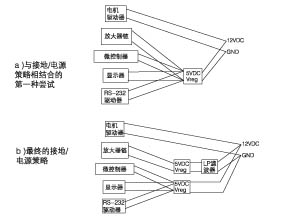



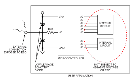
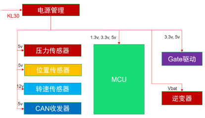
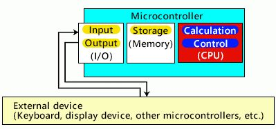


評論