Analyzing noise from the perspective of portable-system design will help you in making appropriate trade-off in power-supply design.
RF-communicating computers and other new mobile systems can act as portable generators of unwanted noise and EMI, thereby hampering their own market acceptance. Witness the near disaster at New York's La Guardia Airport, in which EMI from a notebook computer may have caused a failure in an airliner's landing system. Or, consider the first DOS palmtop computers, which vibrated so much from audible switching-regulator noise that the computers could "walk" right off the table.
Problems with power-supply noise are seldom as dramatic as these cases. Instead, system designers usually resolve problems during the R&D phase; end users indirectly, if at all, see problems only as delays in the product's introduction.
Noise is particularly interesting for portable systems, because the power supply is often a custom design, created by the same team responsible for the logic board, analog circuitry, and other subsystems. For a portable system, then, you can't just procure the power supply as a black box with guaranteed specifications of maximum output-noise levels.
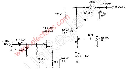
The gate-bias generator for a GaAs MESFET offers a good example of low-noise requirements in a power supply. A typical GaAs transmitter employs the depletion-mode MESFET in a common-source configuration, so the gate needs a negative bias voltage. Any noise on this voltage mixes with the RF signal and produces undesirable intermodulation products, which, in turn, produce unwanted AM sidebands on the RF carrier. The AM bands are impossible to filter if they fall within the RF channel, so you must first specify a clean DC-bias voltage.
Output noise is voltage noise that might upset noise-sensitive loads such as Creative Labs' (Milpitas, CA) SoundBlaster audio electronics. Radiated noise can be electromagnetic or electrostatic and usually originates in magnetic components, such as transformers and inductors, in switches and rectifiers, or at switching nodes that have large, fast voltage swings.
Microphonic noise is audible sound, the usual cause of which is low-frequency switching waveforms that excite coil windings and cause them to vibrate against each other mechanically. You can usually solve this problem by raising the minimum frequency or by applying varnish to the windings.
The worst noise generator in a portable system is almost never the power supply itself. From the power-supply designer's perspective, a notebook computer, for instance, comprises a battery, the power electronics, and many relatively unimportant loads, such as the CPU, the RAM, and the I/O. From this power-centric viewpoint, the CPU is a big heat source that generates lots of noise and EMI.
Pointing an EMI sniffer at a typical portable unit usually reveals the system clock as the worst noise signal, with power-supply noise comparably much lower. This relative importance also applies to conducted noise; the switching noise induced by dynamic load changes in a clocked-CMOS logic system usually produces far more voltage noise on the supply rails than does the switcher itself. Start-stop clock operation, which presents the power supply with brutal 50A/msec load transients, produces particularly troublesome voltage noise.
Who's to blame when the load induces noise on the supply rails? Logic designers can easily blame the power-supply designers by saying "if the wretched power supply had lower output impedance, all my logic noise would shunt to ground, and everyone would be happy." The point is that load-induced noise is a system-design issue. To ensure that everyone is happy, including the purchasing department, logic and power-supply designers must cooperate.
Start-stop clock operation illustrates this need for cooperation. The usual brute-force method for curing Ldi/dt spikes, which large-load transients cause, is expensive: Connect low-impedance bypass capacitors across the load, making the transients smaller and slower by the time they reach the power supply. This method works, but other approaches can be more cost-effective and space-efficient.
If, for example, the DC output tolerance is tighter, say,±2% instead of ±5%, then the Ldi/dt dip and overshoot need not carry VOUT beyond limits that the logic can tolerate. In other words, a tighter tolerance on the voltage reference can improve the system by reducing the size and the cost of filter capacitors.
Simplicity and high efficiency are why the buck and boost topologies are extremely common in portable systems. Buck and boost configurations are almost mirror images of each other, which makes them useful for illustrating noise issues in DC/DC converters. Buck and boost topologies are closely related. If you connect a voltage source across its output and a load resistor across its input, a buck regulator with a synchronous rectifier operates backward as a boost converter and steps up the voltage.
The power inductor in a switch-mode regulator can sometimes act as a filter for the chopped-current waveforms that the switching action produces. For buck circuits, the inductor filters current into the output-filter capacitor. For boost circuits, the inductor filters current coming from the input- filter capacitor. Thus, the buck regulator has a relatively quiet output, and the boost regulator has a relatively quiet input (Figure 1). The two topologies are duals, because one is the inverse of the other. By choosing the battery voltage (low versus high) for a given application, you can opt for the circuit topology that minimizes noise at the more sensitive location.
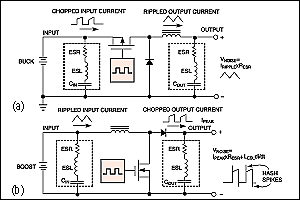
Figure 1. By choosing either a buck (a) or boost (b) regulator, which are the inverse of each other, you can select the location of the predominant noise. Buck regulators have a noisy input and quiet output; boost regulators have a quiet input and noisy output.
Output noise is more important than input noise if the system has a noise-sensitive load. For such systems, a buck-converter application reaps the benefit of benign inductor-current waveforms. Lacking sharp current steps, these waveforms don't produce high-frequency output-noise spikes. Some other switching-regulator topologies do create these spikes, because the waveforms interact with the trace inductance and the effective series inductance (ESL) of the capacitor. Any "hash" noise (very high-frequency noise spikes) at the output of a buck converter is probably just phantom noise that the ground lead of your scope probe produces by picking up EMI. Stray capacitance at the switching node introduces second-order effects that can also result in output hash, but this effect is usually imperceptible.
Phantom noise doesn't exist at the point of measurement until you attach a scope probe; but this noise warrants concern, because EMI can get into sensitive circuitry as easily as it gets into the probe's ground lead. You can reduce susceptibility to EMI by slowing the rise and fall times of the switching waveform and by lowering the inductance of paths that carry substantial amounts of switched current. To eliminate phantom noise entirely, however, you must shield the sensitive circuitry with steel or mu-metal, but not copper.
Operating a buck converter in its deep continuous-conduction mode, in which the inductor current does not return to zero within each switching cycle, further reduces the output noise by lowering the amplitude of ripple current. You obtain continuous conduction by increasing the inductance value. Thus, the penalties include a larger inductor, lower efficiency due to I2R loss in the greater number of windings, and a slower response to load transients because of the larger inductor's lower current-slew rate.
You can easily suppress these high-frequency spikes, which often reach hundreds of millivolts in amplitude, with a simple RC filter in the supply line, such as a 0.1(ohm) resistor in series and a 0.1μF ceramic capacitor to ground. Often, the parasitic inductance of wires connecting the power supply and load is enough to quash these hash spikes.
Input-current noise not suppressed by the input filter capacitor (due to excessive ESR and ESL associated with the input capacitor) returns to the battery and AC adapter. This same noise can then pollute other loads connected to the battery. If noise causes the battery wire or AC-adapter cable to act as an antenna, the resulting EMI can possibly violate FCC regulations.
The input-filter capacitor in a buck-topology regulator is subject to large current steps; in a boost circuit, this capacitor's current comprises gentle ramps. Compared with triangle waves in the boost case, the chopped, square-wave input currents of a buck regulator have high initial amplitudes and include high-frequency components that can cause RFI. Fourier analysis shows that square-wave harmonics roll off at 20dB per decade, versus 40dB per decade for the triangle waves. Unfortunately, the other two topologies in common use for portable systems, buck-boost and flyback, both have chopped-ripple waveforms at the input and the output.
Parasitic inductance and resistance in the output filter capacitor is the main cause of voltage noise at the output of a switch-mode regulator. A secondary cause of output noise is the finite value of that capacitor. Current pulses, those that either the regulator injects or that digital switching noise in the load induces, interact with the capacitor's ESR and ESL to produce voltage steps and spikes (Figure 2).
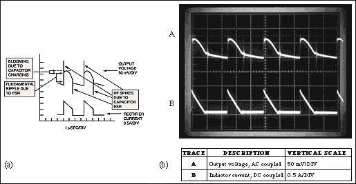
Figure 2. Ripple current at the switched-mode regulator's switching frequency causes ESR-induced noise steps. Fast-rising current edges cause ESL-induced hash spikes (a). The photo in (b) clearly shows the effects of ESR and capacitance, but the ESL-induced high-frequency spikes aren't visible. This 175kHz, 5V to 12V converter operates in the discontinuous mode, so the ESR steps exist only at leading edges of the triangular current waveform.
ESR-induced noise follows ohm's law: peak-to-peak noise equals ESR times the current-pulse amplitudes. ESL-induced noise has an amplitude that is proportional to the product of ESL and the rate of change of the current-pulse edges. For example, if you inject a 1A pulse with a 20nsec rise time into a tantalum capacitor, whose ESL is typically 4nH, the result is a sharp Ldi/dt spike of 4nHx(1A/20nsec) = 200mV.
The switching noise also has a capacitive component that causes a blooming effect: Fast-slewing inductor current dumps into the output and then decays in an RC fashion during the second half of the switching cycle, as the output capacitor discharges into the load. The amount of charge dumped with each cycle and the capacity of the filter determine the amount of capacitive blooming and decay. This capacitive ripple is generally less obvious than the ESR and ESL effect, because typical electrolytic and tantalum power-supply capacitors have relatively large amounts of capacitance for a given level of ESR and ESL.
In other words, resistance and inductance rather than capacitance dominate the capacitor's AC impedance at the switching frequency. However, as designers begin to employ switching frequencies of 500kHz and greater and, as a result, move to ceramic-filter capacitors, this rule is changing. Compared with aluminum electrolytic and tantalum capacitors, the ceramic types have less capacitance for a given cost and size. Also, reducing capacitance, given the same amount of charge, results in larger voltage changes.
As an ultimate noise squasher, many designers keep in their toolbox a monster capacitor, such as the Sanyo OS-CON 2200μF, organic-semiconductor, solid-aluminum device (with about 5m(ohm) of ESR), or a 100μF multilayer ceramic capacitor for high-frequency duty. These specialized capacitors make great noise killers, owing more to their ultra-low ESR and ESL than to their large capacitance. For comparison, a 220μF, 10V AVX TPS surface-mount tantalum capacitor has about a 60m(ohm) ESR and 4nH ESL, and a 1μF monolithic ceramic capacitor has about a 10m(ohm) ESR and 100pH ESL.
Aside from imperfections in the filter capacitor, the main cause of output noise in a switching regulator is the circuit topology and operating point. The net effect of the inductance, the ratio of input and output voltages, and the switching frequency determine the amplitude and the shape of current pulses being dumped into the output.
The control loop of a switch-mode regulator typically has only a secondary effect on the regulator's output noise. Current-mode PWM control, for example, has a noise characteristic very similar to that of duty-ratio (voltage-mode) PWM. This rule does have some glaring exceptions. In simple hysteretic feedback loops, the output ripples between two comparator-threshold voltages, and in pulse-skipping pulse-frequency-modulated (PFM) regulators the switching frequency is a function of load current.
An unstable control loop can also cause an increase in output noise. For example, a current-mode PWM regulator that has improper slope compensation exhibits a staircase inductor-current waveform whose peak currents exceed the normal levels, as determined by operating conditions. These peak currents then flow through the output-capacitor ESR, causing high levels of ripple voltage.
Observing the output-noise waveform of a switching regulator on an oscilloscope can reveal a lot about the regulator's operation. The effect of ESR usually dominates the output noise, so the voltage ripple mirrors the inductor-current waveform. With practice, you can identify operating parameters, such as duty ratio, inductor saturation, discontinuous operation, and current-mode inner-loop instability, without connecting a current probe or inserting a current-sense resistor in series with the inductor or the transformer.
Fixed-frequency PWM (Figure 3, c and d) provides the most stable and predictable noise performance of any control architecture. You can choose the switching frequency and its harmonics such that the audio band or a selected RF band remains free of switching noise. For demanding applications, you can eliminate error and drift in the oscillator frequency by synchronizing the PWM controller to an external clock. Not all PWM architectures have a fixed frequency; the hysteretic and constant-off-time architectures are variable-frequency types.
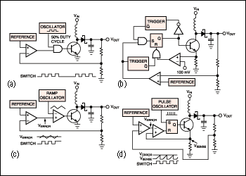
Figure 3. Though somewhat noisier than PWM converters, pulse-skipping PFM converters, such as the clocked (a) and hysteretic (b) types, have extremely high light-load efficiency, making them popular for battery-powered systems. PFM converters reduce switching loss by dropping pulses when lightly loaded. PWM converters, such as the duty-ratio-controlled voltage-mode converter in (c) and the current-mode converter in (d), generally switch at a constant frequency.
Variable-frequency PFM is in vogue, because it extends battery life in the suspend and standby modes of operation. At light loads, a PFM system minimizes switching loss by switching at a very low frequency. These low frequencies cause switching noise to dip into the audio band. This low-frequency noise is unwelcome, because low-frequency filters require large and expensive LC components.
Moreover, some designers don't like PFM converters, because the feedback loops of these converters are inherently unstable. This point raises some interesting considerations, such as the relationship between stability and noise. You must ask whether unstable converters are inherently noisier than stable ones. You must also define stability. Some of the criteria for stability are 50° of margin on a gain/phase plot, clean and regular switching waveforms that an oscilloscope can easily trigger on, and VOUT that doesn't overshoot or exceed the allowable output tolerance when you subject the supply voltage to large line and load transients. A PFM or hysteretic-PWM regulator can meet all of these common criteria and still be unstable, yet the instability is not necessarily a problem, except in the most demanding applications.
In the strictest sense, you must regard as unstable a power supply that is stable everywhere but in the frequency domain. Such a rigid definition of stability is useful to audio and RF designers, who must live with the conducted and radiated by-products of power-supply operation. These by-products include noise harmonics at multiples of the fundamental switching frequency. RF-modem designers, for instance, are unhappy if load variations position the PFM supply's variable-switching frequency in such a way that subharmonics fall within the 455kHz IF band.
PFM converters and other unstable converters are generally noisier both in amplitude and frequency than are stable ones. The reasons for this higher noise depend on the converter's design and problem. PFM converters, for example, dump a fixed amount of current into the output at the beginning of each switching cycle. Therefore, even at light loads, the output capacitor gets hit with large-amplitude current pulses. By adding another filter capacitor, you can easily quash the resulting noise amplitude, which is usually 25% to 100% higher than that of a PWM converter. PWM converters, on the other hand, don't allow the peak inductor current to approach the current-limit threshold unless an overload or other fault is present. Instead, a PWM converter's continuously variable duty cycle causes the peak current to hover around some intermediate level that's proportional to the load current.
PFM is inferior to PWM in the frequency domain. You can often, however, select component values that force the PFM converter to operate above the audio band at the minimum load condition (Figure 4). For example, reducing a PFM regulator's maximum on-time by adjusting the timing capacitor of a one shot can raise the minimum switching frequency. The only penalty of this approach is a slight drop in efficiency due to higher switching losses.
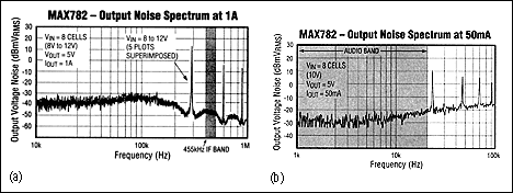
Figure 4. When heavily loaded, the MAX782 battery-powered DC/DC converter operates as a fixed-frequency PWM, concentrating its noise at the 300kHz fundamental switching frequency and associated harmonics (a). At lighter loads, the circuit automatically switches to PFM mode. Then, a judicious selection of components keeps the switching noise above 20kHz for all loads greater than 50mA (b).
From the standpoint of FCC/VDE certification, the randomly variable frequency spectrum of a PFM regulator is preferable to the fixed switching frequency of a PWM regulator. The FCC looks for noise above certain levels in specified frequency bands. A fixed-frequency PWM converter generates noise peaks at the switching frequency and its harmonics, but the randomized noise from a PFM converter usually spreads over a wider range of frequencies.
Recent battery-powered switching regulators can operate as fixed-frequency PWM converters or as pulse-skipping PFM converters, depending on the load current. One such example is IC1 in Figure 5, which takes this concept one step further. This IC provides a noise-suppression control input, SKIP, which overrides the normal, automatic switchover between PFM and PWM modes. Instead, SKIP forces the fixed-frequency operation, regardless of load. Thus, the system must pull SKIP low when activating a noise-sensitive load, such as an RF transmitter.
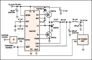
Figure 5. This current-mode PWM controller IC has two low-noise features: an input for synchronizing the internal oscillator with an external clock, and a mode-control input (SKIP) that can override the normal automatic switchover between PWM and PFM, thereby forcing a fixed-frequency continuous-conduction operation even with no load.
A similar version of this article appeared in the January 18, 1996 issue of EDN.
RF-communicating computers and other new mobile systems can act as portable generators of unwanted noise and EMI, thereby hampering their own market acceptance. Witness the near disaster at New York's La Guardia Airport, in which EMI from a notebook computer may have caused a failure in an airliner's landing system. Or, consider the first DOS palmtop computers, which vibrated so much from audible switching-regulator noise that the computers could "walk" right off the table.
Problems with power-supply noise are seldom as dramatic as these cases. Instead, system designers usually resolve problems during the R&D phase; end users indirectly, if at all, see problems only as delays in the product's introduction.
Noise is particularly interesting for portable systems, because the power supply is often a custom design, created by the same team responsible for the logic board, analog circuitry, and other subsystems. For a portable system, then, you can't just procure the power supply as a black box with guaranteed specifications of maximum output-noise levels.
The gate-bias generator for a GaAs MESFET offers a good example of low-noise requirements in a power supply. A typical GaAs transmitter employs the depletion-mode MESFET in a common-source configuration, so the gate needs a negative bias voltage. Any noise on this voltage mixes with the RF signal and produces undesirable intermodulation products, which, in turn, produce unwanted AM sidebands on the RF carrier. The AM bands are impossible to filter if they fall within the RF channel, so you must first specify a clean DC-bias voltage.
Types of Noise
Noise in portable systems takes several forms. The major types are input, output, radiated, and microphonic. Input noise generally comprises reflected ripple, in which the input-current noise of a switch-mode power supply interacts with the source impedance of the raw supply voltage. Combined with any RF noise, which can be induced by high-speed logic and coupled back through the power supply to the input, the resultant disturbance can pollute the AC-line and battery voltages.Output noise is voltage noise that might upset noise-sensitive loads such as Creative Labs' (Milpitas, CA) SoundBlaster audio electronics. Radiated noise can be electromagnetic or electrostatic and usually originates in magnetic components, such as transformers and inductors, in switches and rectifiers, or at switching nodes that have large, fast voltage swings.
Microphonic noise is audible sound, the usual cause of which is low-frequency switching waveforms that excite coil windings and cause them to vibrate against each other mechanically. You can usually solve this problem by raising the minimum frequency or by applying varnish to the windings.
The worst noise generator in a portable system is almost never the power supply itself. From the power-supply designer's perspective, a notebook computer, for instance, comprises a battery, the power electronics, and many relatively unimportant loads, such as the CPU, the RAM, and the I/O. From this power-centric viewpoint, the CPU is a big heat source that generates lots of noise and EMI.
Pointing an EMI sniffer at a typical portable unit usually reveals the system clock as the worst noise signal, with power-supply noise comparably much lower. This relative importance also applies to conducted noise; the switching noise induced by dynamic load changes in a clocked-CMOS logic system usually produces far more voltage noise on the supply rails than does the switcher itself. Start-stop clock operation, which presents the power supply with brutal 50A/msec load transients, produces particularly troublesome voltage noise.
Who's to blame when the load induces noise on the supply rails? Logic designers can easily blame the power-supply designers by saying "if the wretched power supply had lower output impedance, all my logic noise would shunt to ground, and everyone would be happy." The point is that load-induced noise is a system-design issue. To ensure that everyone is happy, including the purchasing department, logic and power-supply designers must cooperate.
Start-stop clock operation illustrates this need for cooperation. The usual brute-force method for curing Ldi/dt spikes, which large-load transients cause, is expensive: Connect low-impedance bypass capacitors across the load, making the transients smaller and slower by the time they reach the power supply. This method works, but other approaches can be more cost-effective and space-efficient.
If, for example, the DC output tolerance is tighter, say,±2% instead of ±5%, then the Ldi/dt dip and overshoot need not carry VOUT beyond limits that the logic can tolerate. In other words, a tighter tolerance on the voltage reference can improve the system by reducing the size and the cost of filter capacitors.
Topology Trade-Off
The topology of a switch-mode supply, its configuration of connections among the switches and energy-storage elements, has a strong effect on the output noise. For portable systems, the topology of choice for a battery-input power supply is usually one of the five basic types: buck (step-down), boost (step-up), buck-boost, flyback, or Royer.Simplicity and high efficiency are why the buck and boost topologies are extremely common in portable systems. Buck and boost configurations are almost mirror images of each other, which makes them useful for illustrating noise issues in DC/DC converters. Buck and boost topologies are closely related. If you connect a voltage source across its output and a load resistor across its input, a buck regulator with a synchronous rectifier operates backward as a boost converter and steps up the voltage.
The power inductor in a switch-mode regulator can sometimes act as a filter for the chopped-current waveforms that the switching action produces. For buck circuits, the inductor filters current into the output-filter capacitor. For boost circuits, the inductor filters current coming from the input- filter capacitor. Thus, the buck regulator has a relatively quiet output, and the boost regulator has a relatively quiet input (Figure 1). The two topologies are duals, because one is the inverse of the other. By choosing the battery voltage (low versus high) for a given application, you can opt for the circuit topology that minimizes noise at the more sensitive location.

Figure 1. By choosing either a buck (a) or boost (b) regulator, which are the inverse of each other, you can select the location of the predominant noise. Buck regulators have a noisy input and quiet output; boost regulators have a quiet input and noisy output.
Output noise is more important than input noise if the system has a noise-sensitive load. For such systems, a buck-converter application reaps the benefit of benign inductor-current waveforms. Lacking sharp current steps, these waveforms don't produce high-frequency output-noise spikes. Some other switching-regulator topologies do create these spikes, because the waveforms interact with the trace inductance and the effective series inductance (ESL) of the capacitor. Any "hash" noise (very high-frequency noise spikes) at the output of a buck converter is probably just phantom noise that the ground lead of your scope probe produces by picking up EMI. Stray capacitance at the switching node introduces second-order effects that can also result in output hash, but this effect is usually imperceptible.
Phantom noise doesn't exist at the point of measurement until you attach a scope probe; but this noise warrants concern, because EMI can get into sensitive circuitry as easily as it gets into the probe's ground lead. You can reduce susceptibility to EMI by slowing the rise and fall times of the switching waveform and by lowering the inductance of paths that carry substantial amounts of switched current. To eliminate phantom noise entirely, however, you must shield the sensitive circuitry with steel or mu-metal, but not copper.
Operating a buck converter in its deep continuous-conduction mode, in which the inductor current does not return to zero within each switching cycle, further reduces the output noise by lowering the amplitude of ripple current. You obtain continuous conduction by increasing the inductance value. Thus, the penalties include a larger inductor, lower efficiency due to I2R loss in the greater number of windings, and a slower response to load transients because of the larger inductor's lower current-slew rate.
Chopped-Current Waveforms Produce Noise
The output capacitor of a boost converter is subject to abrupt current steps equal to the entire peak inductor current, rather than just the ripple component, because the rectifier diode chops the inductor current. These high-amplitude fast-moving current transitions can generate some noise when they interact with the ESL and equivalent series resistance (ESR) of the output capacitor. In addition to large voltage steps that ESR causes, the ESL causes tiny, high-frequency hash spikes at the leading and trailing edges of the switching waveform.You can easily suppress these high-frequency spikes, which often reach hundreds of millivolts in amplitude, with a simple RC filter in the supply line, such as a 0.1(ohm) resistor in series and a 0.1μF ceramic capacitor to ground. Often, the parasitic inductance of wires connecting the power supply and load is enough to quash these hash spikes.
Input-current noise not suppressed by the input filter capacitor (due to excessive ESR and ESL associated with the input capacitor) returns to the battery and AC adapter. This same noise can then pollute other loads connected to the battery. If noise causes the battery wire or AC-adapter cable to act as an antenna, the resulting EMI can possibly violate FCC regulations.
The input-filter capacitor in a buck-topology regulator is subject to large current steps; in a boost circuit, this capacitor's current comprises gentle ramps. Compared with triangle waves in the boost case, the chopped, square-wave input currents of a buck regulator have high initial amplitudes and include high-frequency components that can cause RFI. Fourier analysis shows that square-wave harmonics roll off at 20dB per decade, versus 40dB per decade for the triangle waves. Unfortunately, the other two topologies in common use for portable systems, buck-boost and flyback, both have chopped-ripple waveforms at the input and the output.
Parasitic inductance and resistance in the output filter capacitor is the main cause of voltage noise at the output of a switch-mode regulator. A secondary cause of output noise is the finite value of that capacitor. Current pulses, those that either the regulator injects or that digital switching noise in the load induces, interact with the capacitor's ESR and ESL to produce voltage steps and spikes (Figure 2).

Figure 2. Ripple current at the switched-mode regulator's switching frequency causes ESR-induced noise steps. Fast-rising current edges cause ESL-induced hash spikes (a). The photo in (b) clearly shows the effects of ESR and capacitance, but the ESL-induced high-frequency spikes aren't visible. This 175kHz, 5V to 12V converter operates in the discontinuous mode, so the ESR steps exist only at leading edges of the triangular current waveform.
ESR-induced noise follows ohm's law: peak-to-peak noise equals ESR times the current-pulse amplitudes. ESL-induced noise has an amplitude that is proportional to the product of ESL and the rate of change of the current-pulse edges. For example, if you inject a 1A pulse with a 20nsec rise time into a tantalum capacitor, whose ESL is typically 4nH, the result is a sharp Ldi/dt spike of 4nHx(1A/20nsec) = 200mV.
The switching noise also has a capacitive component that causes a blooming effect: Fast-slewing inductor current dumps into the output and then decays in an RC fashion during the second half of the switching cycle, as the output capacitor discharges into the load. The amount of charge dumped with each cycle and the capacity of the filter determine the amount of capacitive blooming and decay. This capacitive ripple is generally less obvious than the ESR and ESL effect, because typical electrolytic and tantalum power-supply capacitors have relatively large amounts of capacitance for a given level of ESR and ESL.
In other words, resistance and inductance rather than capacitance dominate the capacitor's AC impedance at the switching frequency. However, as designers begin to employ switching frequencies of 500kHz and greater and, as a result, move to ceramic-filter capacitors, this rule is changing. Compared with aluminum electrolytic and tantalum capacitors, the ceramic types have less capacitance for a given cost and size. Also, reducing capacitance, given the same amount of charge, results in larger voltage changes.
As an ultimate noise squasher, many designers keep in their toolbox a monster capacitor, such as the Sanyo OS-CON 2200μF, organic-semiconductor, solid-aluminum device (with about 5m(ohm) of ESR), or a 100μF multilayer ceramic capacitor for high-frequency duty. These specialized capacitors make great noise killers, owing more to their ultra-low ESR and ESL than to their large capacitance. For comparison, a 220μF, 10V AVX TPS surface-mount tantalum capacitor has about a 60m(ohm) ESR and 4nH ESL, and a 1μF monolithic ceramic capacitor has about a 10m(ohm) ESR and 100pH ESL.
Aside from imperfections in the filter capacitor, the main cause of output noise in a switching regulator is the circuit topology and operating point. The net effect of the inductance, the ratio of input and output voltages, and the switching frequency determine the amplitude and the shape of current pulses being dumped into the output.
The control loop of a switch-mode regulator typically has only a secondary effect on the regulator's output noise. Current-mode PWM control, for example, has a noise characteristic very similar to that of duty-ratio (voltage-mode) PWM. This rule does have some glaring exceptions. In simple hysteretic feedback loops, the output ripples between two comparator-threshold voltages, and in pulse-skipping pulse-frequency-modulated (PFM) regulators the switching frequency is a function of load current.
An unstable control loop can also cause an increase in output noise. For example, a current-mode PWM regulator that has improper slope compensation exhibits a staircase inductor-current waveform whose peak currents exceed the normal levels, as determined by operating conditions. These peak currents then flow through the output-capacitor ESR, causing high levels of ripple voltage.
Observing the output-noise waveform of a switching regulator on an oscilloscope can reveal a lot about the regulator's operation. The effect of ESR usually dominates the output noise, so the voltage ripple mirrors the inductor-current waveform. With practice, you can identify operating parameters, such as duty ratio, inductor saturation, discontinuous operation, and current-mode inner-loop instability, without connecting a current probe or inserting a current-sense resistor in series with the inductor or the transformer.
Pulse-Skipping PFM versus PWM Control Schemes
Although PFM control has become prevalent in battery-operated equipment because its light-load efficiency exceeds that of PWM, the actual PFM operation is less well known (Figure 3, a and b). PFM is worth examining, because this scheme showcases some important issues concerning stability and frequency-domain effects.Fixed-frequency PWM (Figure 3, c and d) provides the most stable and predictable noise performance of any control architecture. You can choose the switching frequency and its harmonics such that the audio band or a selected RF band remains free of switching noise. For demanding applications, you can eliminate error and drift in the oscillator frequency by synchronizing the PWM controller to an external clock. Not all PWM architectures have a fixed frequency; the hysteretic and constant-off-time architectures are variable-frequency types.

Figure 3. Though somewhat noisier than PWM converters, pulse-skipping PFM converters, such as the clocked (a) and hysteretic (b) types, have extremely high light-load efficiency, making them popular for battery-powered systems. PFM converters reduce switching loss by dropping pulses when lightly loaded. PWM converters, such as the duty-ratio-controlled voltage-mode converter in (c) and the current-mode converter in (d), generally switch at a constant frequency.
Variable-frequency PFM is in vogue, because it extends battery life in the suspend and standby modes of operation. At light loads, a PFM system minimizes switching loss by switching at a very low frequency. These low frequencies cause switching noise to dip into the audio band. This low-frequency noise is unwelcome, because low-frequency filters require large and expensive LC components.
Moreover, some designers don't like PFM converters, because the feedback loops of these converters are inherently unstable. This point raises some interesting considerations, such as the relationship between stability and noise. You must ask whether unstable converters are inherently noisier than stable ones. You must also define stability. Some of the criteria for stability are 50° of margin on a gain/phase plot, clean and regular switching waveforms that an oscilloscope can easily trigger on, and VOUT that doesn't overshoot or exceed the allowable output tolerance when you subject the supply voltage to large line and load transients. A PFM or hysteretic-PWM regulator can meet all of these common criteria and still be unstable, yet the instability is not necessarily a problem, except in the most demanding applications.
In the strictest sense, you must regard as unstable a power supply that is stable everywhere but in the frequency domain. Such a rigid definition of stability is useful to audio and RF designers, who must live with the conducted and radiated by-products of power-supply operation. These by-products include noise harmonics at multiples of the fundamental switching frequency. RF-modem designers, for instance, are unhappy if load variations position the PFM supply's variable-switching frequency in such a way that subharmonics fall within the 455kHz IF band.
PFM converters and other unstable converters are generally noisier both in amplitude and frequency than are stable ones. The reasons for this higher noise depend on the converter's design and problem. PFM converters, for example, dump a fixed amount of current into the output at the beginning of each switching cycle. Therefore, even at light loads, the output capacitor gets hit with large-amplitude current pulses. By adding another filter capacitor, you can easily quash the resulting noise amplitude, which is usually 25% to 100% higher than that of a PWM converter. PWM converters, on the other hand, don't allow the peak inductor current to approach the current-limit threshold unless an overload or other fault is present. Instead, a PWM converter's continuously variable duty cycle causes the peak current to hover around some intermediate level that's proportional to the load current.
PFM is inferior to PWM in the frequency domain. You can often, however, select component values that force the PFM converter to operate above the audio band at the minimum load condition (Figure 4). For example, reducing a PFM regulator's maximum on-time by adjusting the timing capacitor of a one shot can raise the minimum switching frequency. The only penalty of this approach is a slight drop in efficiency due to higher switching losses.

Figure 4. When heavily loaded, the MAX782 battery-powered DC/DC converter operates as a fixed-frequency PWM, concentrating its noise at the 300kHz fundamental switching frequency and associated harmonics (a). At lighter loads, the circuit automatically switches to PFM mode. Then, a judicious selection of components keeps the switching noise above 20kHz for all loads greater than 50mA (b).
Output Noise versus Frequency
The extra noise that a pulse-skipping PFM regulator produces is usually inconsequential, except in demanding applications, such as a tightly packed cellular phone or an 18-bit stereo-sound adapter. Notebook computers and other predominantly digital systems are quite tolerant of power-supply ripple. Moreover, peak currents are benign at the power levels typical in portable systems, so the resulting noise is seldom a headache.From the standpoint of FCC/VDE certification, the randomly variable frequency spectrum of a PFM regulator is preferable to the fixed switching frequency of a PWM regulator. The FCC looks for noise above certain levels in specified frequency bands. A fixed-frequency PWM converter generates noise peaks at the switching frequency and its harmonics, but the randomized noise from a PFM converter usually spreads over a wider range of frequencies.
Recent battery-powered switching regulators can operate as fixed-frequency PWM converters or as pulse-skipping PFM converters, depending on the load current. One such example is IC1 in Figure 5, which takes this concept one step further. This IC provides a noise-suppression control input, SKIP, which overrides the normal, automatic switchover between PFM and PWM modes. Instead, SKIP forces the fixed-frequency operation, regardless of load. Thus, the system must pull SKIP low when activating a noise-sensitive load, such as an RF transmitter.

Figure 5. This current-mode PWM controller IC has two low-noise features: an input for synchronizing the internal oscillator with an external clock, and a mode-control input (SKIP) that can override the normal automatic switchover between PWM and PFM, thereby forcing a fixed-frequency continuous-conduction operation even with no load.
A similar version of this article appeared in the January 18, 1996 issue of EDN.
 電子發(fā)燒友App






評論