Introduction
The DS2751 multichemistry battery fuel gauge has an operating range such that it can be used in singlecell Lithium Ion/Polymer packs or 3-cell Nickel packs. However, many applications necessitate more cells in a series stack. The DS2751 can still be used as a fuel gauging IC in those applications by dividing the multiple cell voltage down to an acceptable level. This method allows the use of all the features of the DS2751 including integrated 25mΩ sense resistor, temperature/voltage/current measurement, current accumulation (coulomb counting), 32-bytes of EEPROM, and a single wire communication interface.Overview
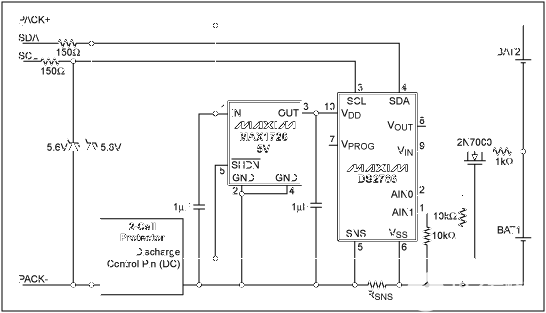
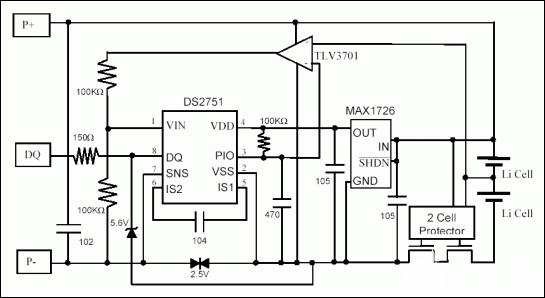
The schematic in Figure 1 illustrates a possible solution for using the DS2751 in a two cell application. Although not required for basic fuel gauging as described in AN131, this circuit presents a method to measure the dual cell voltage. In this application, PIO is used to switch the comparator output to drive one of its supply rails across the resistor dividing network. With PIO low, the voltage at VIN is half of the dual cell voltage, and with PIO high, VIN is 0V. To provide constant power to the DS2751, a low dropout voltage regulator (LDO) is required to step down the dual cell voltage to an acceptable level. A dual cell protector is also necessary to protect the cells from fault conditions. As shown in the schematic, all components for this circuit must reside on the contact side (as opposed to the cell side) of the protector.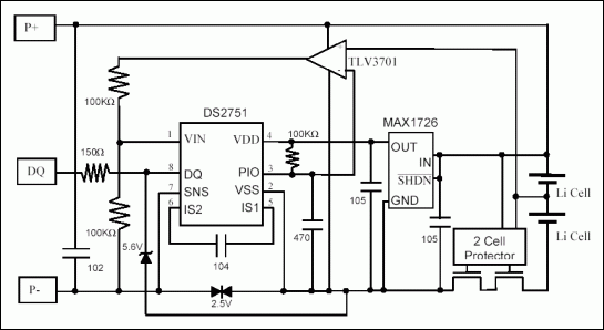
Figure 1. DS2751 in a 2-cell Li+/Polymer battery pack.
Detailed Description
The recommended supply voltage for the DS2751 ranges from 2.5V to 5.5V, so the LDO output voltage must be chosen accordingly. The LDO must also have a low quiescent current and be able to handle the input voltage presented by a multiple cell stack. The MAX1726 with a 5V output satisfies all criteria. It supports a 12V maximum input voltage and draws 2μA of supply current. The 5V output is used because the LDO efficiency decreases as the input voltage increases above the output voltage. With a nominal input voltage of 7.6V, this is the optimum output voltage. The 5V output also ensures that the VDD voltage remains above the VIN voltage for all conditions. To prevent data loss in the DS2751, the SHDN pin of the MAX1726 should be connected to the input voltage as shown in Figure 1. This will ensure the MAX1726 does not enter shutdown mode, which would remove power from the DS2751. The 1μF input and output capacitors are data sheet recommended. Please refer to the MAX1726 data sheet for application specific capacitor selection.The maximum reportable voltage from the DS2751 voltage register (addresses 0Ch and 0Dh) is 4.99V. A dividing scheme is thus necessary to drop the cell stack voltage to a measurable level. For this purpose, two precision 100kΩ resistors are used to divide the stack voltage in half. The constant DC current drain from the resistors would be prohibitive for battery-powered applications, so a comparator is used to switch the current on and off. The TLV3701 nanopower comparator is used for switching because it can withstand supply voltages up to 16V, and lists a 560nA typical supply current. The DS2751 open-drain PIO pin is used as the control pin for the comparator switch. The PIO pin automatically changes to a high-impedance state if the DQ line is low for more than 2 seconds, or if the DS2751 enters sleep mode. A 100kΩ pullup resistor to the LDO output ensures that PIO will be a logic high in this state. The other comparator input is connected to the positive terminal of the bottom cell in the stack. This configuration produces a differential voltage at the comparator inputs for both PIO logic levels. The 47pF capacitor from PIO to ground helps to stop negative undershoot when PIO is driven low.
With the comparator output low, the voltage at VIN is 0V. Because of this, the undervoltage sleep enable (UVEN) function must be disabled, or the DS2751 will never transition to active mode. To disable UVEN, a value of 0 is written to bit 3 of address 31h. When a voltage measurement is needed, the PIO bit in the special feature register (bit 6, address 08h) is set to 0 followed by a delay of at least 6.8ms. This delay is necessary for the DS2751 to update the voltage register with the new voltage at the VIN pin. After reading the voltage register, the PIO bit is set back to 1. The total cell stack voltage is calculated by multiplying the voltage register value by 2. Experimental results showed that adding an additional 0.1V to the doubled voltage register value produced a cell stack voltage accurate to 99%. The additional 0.1V is needed to account for the voltage drop from the comparator positive rail to the comparator output.
For protection of the cell stack, any multiple-cell standalone protector supporting NMOS or PMOS FETs can be used. The standalone protector is placed on the cell side of the DS2751, as illustrated in Figure 1. With this configuration, power to all external components will be disconnected via the protection FETs if a fault condition occurs. When the fault condition is corrected, the discharge FET will again be turned on, and all components will be powered up. As long as the UVEN function is disabled, the DS2751 can go to sleep in only one condition: If the PMOD bit is set to 1 (recommended), and DQ is a logic low for > 2s (pack disconnect). This causes the DS2751 to revert to a low power sleep mode and cease temperature, voltage, current, and accumulated current measurements. Reconnecting the pack and pulling DQ high causes the DS2751 to return to active mode.
The configuration shown in Figure 1 assumes an internal 25mΩ sense resistor. Please refer to the DS2751 data sheet for help choosing an appropriate external sense resistor for your application. All other passive components shown in Figure 1 are included for filtering and ESD protection as shown in the DS2751 data sheet.
 電子發(fā)燒友App









評論