Abstract: The DS2760 and DS2761 battery monitor and protector are battery management ICs geared mainly for single-cell Li-Ion battery pack applications. Although designed mainly for use in the single cell applications, these devices can be used in multiple-cell applications. This application note demonstrates to the user how to use the DS2760 or DS2761 in a multiple-cell application including necessary circuit modifications and limitations in functionality of the devices in the multiple-cell environment. An example circuit is shown along with recommended device configuration of the DS2760 or DS2761 battery monitors.
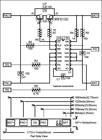
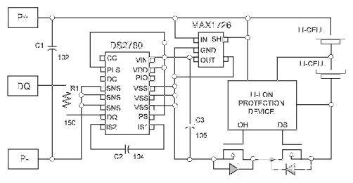
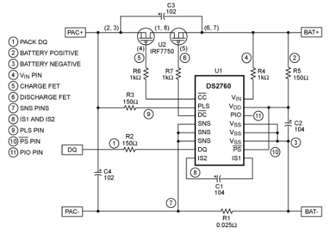
The schematic of Figure 1 illustrates a possible use of the DS2760 in a multi-cell application. The passives connected to the DS2760 are necessary for proper filtering and ESD enhancement, as indicated in the DS2760 datasheet. Please refer to the specification of the specific LDO and protector you are using for recommended schematic. The DS2760/LDO must reside on the contact side (as opposed to the cell side) of the protector, as drawn.

Figure 1. Example schematic of the DS2760 in a 2-cell Li-Ion/Polymer battery pack.
Introduction
The DS2760 High Precision Li-Ion Battery Monitor has an operating range such that it can be used in single-cell Li-Ion or Li-Polymer packs or 2- or 3-cell Ni packs. Many applications however necessitate more cells in the series stack. The DS2760 can be used as a fuel gauge IC in those applications, thereby taking advantage of the many features of the DS2760 including integrated 25mΩ sense resistor, temperature/voltage/current measurement, current accumulation (coulomb counting), 32-bytes EEPROM, and a single wire communication interface. The only features of the DS2760 that cannot be utilized in a multi-cell application are the integrated protector in Li packs and the SWAP function. This application note addresses use of the DS2760 in multi-cell applications with an external protector such as the Mitsumi MM1292 for 2-cell Li packs.The schematic of Figure 1 illustrates a possible use of the DS2760 in a multi-cell application. The passives connected to the DS2760 are necessary for proper filtering and ESD enhancement, as indicated in the DS2760 datasheet. Please refer to the specification of the specific LDO and protector you are using for recommended schematic. The DS2760/LDO must reside on the contact side (as opposed to the cell side) of the protector, as drawn.

Figure 1. Example schematic of the DS2760 in a 2-cell Li-Ion/Polymer battery pack.
Description
With the recommended supply voltage range of the DS2760, the device must be powered (Vdd) by an LDO with an output voltage from 3.0V to 4.0V, such as the Maxim MAX1726EUK33. The schematic in Figure 1 assumes that a DS2760 is being used that contains the internal 25mΩ current sense resistor. Otherwise, a low impedance external sense resistor would be required between the SNS and VSS nodes of the DS2760. Refer to the DS2760 datasheet on choosing an appropriate external sense resistor for your application. The schematic of Figure 1 is nearly identical to that recommended in the DS2760 datasheet for single-cell applications. The following contains a list of differences to the schematic and recommended device configuration from the datasheet.- The integrated protector of the DS2760 must not be used in a multiple cell application. Thus, CC and DC should be left floating. Any multiple-cell standalone protector can be used, supporting either NMOS or PMOS FETs. The standalone protector must be placed on the cell side of the DS2760, as illustrated in Figure 1.
- The DS2760 power (Vdd) must be supplied by an LDO with output voltage specs from 3.0V to 4.0V over all possible input voltages. This voltage range is narrower than the DS2760 operating range so that the DS2760 will not enter the sleep mode for a protector violation. Capacitor C3 may need to be changed, depending upon the particular LDO chosen (refer to the LDO specification for recommended output capacitance). The LDO VSS and DS2760 VSS should be at the same potential, such that the protector is on the cell side of the DS2760/LDO circuit.
- The SWAP feature of the DS2760 must not be used in this multiple-cell application. SWAP gives control of the charge and discharge FETs to the DS2760, which of course cannot happen in this application. The Swap Enable bit (SWEN, addr 31h, bit 3) must be set to 0 to disable SWAP commands. If the application requires multiple Li+ packs to be used simultaneously, a mechanical switch can be added so that the primary battery pack is physically disconnected when the extended pack is attached.
- With SWAP disabled, the DS2760 in this configuration can go to Sleep in only two conditions. If the PMOD bit is set to 1 (recommended), and DQ is a logic low for >2sec (pack disconnect), the DS2760 will revert to a low power Sleep mode and cease temperature, voltage, current, and accumulated current measurements. Second, the DS2760 will go to Sleep if the LDO output voltage falls below the Undervoltage threshold of the DS2760. The standalone protector will also have an Undervoltage threshold for each cell in the stack, and when that is reached, the discharge FET will be turned off, thereby completely shutting down the DS2760 and LDO. So regardless of whether the DS2760 or the standalone protector detects an Undervoltage, the DS2760 will either revert to a low power Sleep mode or be completely shut down when the cells are depleted.
- When the safety violation is corrected, the discharge FET will again be turned on, and the DS2760 and LDO will be powered up. With PMOD=1, the DS2760 will return to the Active state when the pack is reconnected and DQ is pulled to a logic high. The DS2760 may also be pulled out of Sleep mode if a charger is detected (PLS>VIN). However, this is not possible to detect while using a standalone protector, so this should be disabled by connecting PLS directly to VIN, as is shown in the schematic.
- In all likelihood, DQ will be controlled by a low-voltage microcontroller or ASIC in the host system. If not, a 4V Zener should be connected between the DQ and SNS pins of the DS2760. If one is used, the Zener should be connected on the DS2760 side of R1 so the resistor can provide ESD protection for the Zener as well as the DS2760 DQ I/O.
- Although it was not implemented in the schematic of Figure 1, the Programmable I/O (PIO) pin may be used to sense a logic level or mirror DQ activity (to control a vibrating motor, for example) so long as the I/O specs of the PIO pin are not violated. The absolute max voltage of the PIO pin (with respect to VSS) is +12V.
 電子發燒友App











評論