Abstract: Application Note 403 describes the software considerations when migrating an existing design based on the DS2155 T1/E1/J1 single chip transceiver (SCT) to the DS26401 T1/E1/J1 octal framer. In comparison, the Dallas Semiconductor DS26401 octal framer uses a completely revised architecture, contains eight independent framers, and the device package is only 50% larger in area than the DS2155. While the DS2155 does include an integrated line interface unit (LIU), the DS26401 will seamlessly interface will all Dallas Semiconductor T1/E1/J1 LIU devices. Any designer who is thinking of migrating an existing design to use the DS26401 should read this application note. The application note contains detailed information for software migration such as: register location changes, how individual functions have changed from the DS2155 to the DS26401, and which new functions are available on the DS26401. In the end, the designer should have enough information to easily migrate an existing design to the DS26401.
While the DS2155 is available in 1-port and 4-port devices, the DS26401 is an 8-port device. Each port in these devices is programmed and operates independently of the others.
Base Address + (0x200 x n), where n = 0 to 7 for Ports 1 through 8
The only functions that are shared by all 8 ports are the Global and BERT Functions. The Global Function registers are GCR1, GCR2, GSR1, GSR2 and the IDR register. All addresses are shown in hexadecimal.
NS = not supported
TSYNCC.0: Resynchronize (RESYNC). When toggled from low to high, a resynchronization of the transmit side framer is initiated. Must be cleared and set again for a subsequent resync.
TSYNCC.1: Sync Enable (SYNCE)
0 = Automatic resync enabled
1 = Automatic resync disabled
TSYNCC.2: Transmit Synchronizer Enable (TSEN)
0 = Transmit-Side Synchronizer Disabled
1 = Transmit-Side Synchronizer Enabled
TLS3.0: Loss-of-Frame Synchronization Detect (LOFD). This is a latched bit which is set when the transmit synchronizer is searching for the sync pattern in the incoming data stream.
TLS3.1: Loss of Frame (LOF). A real-time status bit which indicates that the transmit side synchronizer is searching for the synchronization pattern in the incoming data stream.
GCR1.2: Bulk Write Enable (BWE). When this bit is set, a port write to one of the octal ports will be mapped into all eight ports. Useful for device initialization.
0 = Normal operation
1 = Bulk write is enabled
GCR1.3: Reference Clock Frequency Select (REFCLKS). This bit sets the divider ratio of the internal clock generator depending on the frequency of the reference clock input.
0 = REF_CLK is 1.544MHz
1 = REF_CLK is 2.048MHz
GCR1.4: Ganged IBO Enable (GIBO). This bit is used to select either the internal MUX for IBO operation or externally "wire-or" operation. Normally this bit should be set = 0 and the internal MUX used.
0 = Use internal IBO mux.
1 = Externally "wire-or" TSER pins and RSER pins for IBO operation.
GCR1.5: Receive Loss-of-Frame/Loss-of-Transmit Clock indication Select (RLOFLTS)
0 = RLOF/LOTCx pins indicate receive loss of frame
1 = RLOF/LOTCx pins indicate loss of transmit clock
GCR1.6: BERT Loss-of-Sync Interrupt Mask (BLOSIM)
0 = DS26401 will not generate an interrupt on INT for a BERT LOS
1 = DS26401 will generate an interrupt on INT for a BERT LOS
GCR1.7: BERT Bit Error Detect Interrupt Mask (BBEDIM)
0 = DS26401 will not generate an interrupt on INT for a BERT bit error detect
1 = DS26401 will generate an interrupt on INT for a BERT bit error detect
GCR2. 0: Receive Channel Block/Clock Select (RCBCS)
This bit controls the function of all eight RCHBLK/CLK pins.
0 = RCHBLK/CLK pins output RCHBLK(1-8) (Receive Channel Block)
1 = RCHBLK/CLK pins output RCHCLK(1-8) (Receive Channel Clock)
GCR2.1: Transmit Channel Block/Clock Select (TCBCS).
This bit controls the function of all eight TCHBLK/CLK pins.
0 = TCHBLK/CLK pins output TCHBLK(1-8) (Transmit Channel Block)
1 = TCHBLK/CLK pins output TCHCLK(1-8) (Transmit Channel Clock)
GCR2.2: Receive Frame/Multiframe Sync Select (RFMSS).
This bit controls the function of all eight RF/RMSYNC pins.
0 = RF/RMSYNC pins output RFSYNC(1-8) (Receive Frame Sync)
1 = RF/RMSYNC pins output RMSYNC(1-8) (Receive Multiframe Sync)
GCR2.3: Receive Loss-of-Signal/Signaling Freeze Select (RLOSSFS). This bit controls the function of all eight RLOS/RSIGF pins.
0 = RLOS/RSIGF pins output RLOS(1-8) (receive loss of signal)
1 = RLOS/RSIGF pins output RSIGF(1-8) (receive signaling freeze)
GCR2.6 and GCR2.7: Interleave Bus Operation Mode Select 0-1 (IBOMS0/1). These bits determine the configuration of the IBO (interleaved bus) multiplexer. These bits should be with the Rx and Tx IBO control registers within each of the framer units. Additional information concerning the IBO mux is given in the data sheet.
RCR.1: Receive RAI Integration Enable (RAIIE). In T1 ESF mode, the RAI indication can be interrupted for a period not to exceed 100ms per interruption as stated in ANSI T1.403. In T1 ESF mode, setting RAIIE will cause the RAI status from the DS26401 to be integrated for 200ms.
0 = RAI detects when 16 consecutive patterns of 00FF appear in the FDL. RAI clears when 14 or less patterns of 00FF hex out of 16 possible appear in the FDL
1 = RAI detects when the condition has been present for greater than 200ms. RAI clears when the condition has been absent for greater than 200ms.
RCR3.7: Input Data Format (IDF)
0 = Bipolar data is expected at RPOS and RNEG (either AMI or B8ZS)
1 = NRZ data is expected at RPOS. The BPV counter will be disabled and RNEG will be ignored by the DS26401.
RRTS1.0: Receive Loss-of-Frame Condition (RLOF). Set when the DS26401 is not synchronized to the received data stream.
RRTS1.1: Receive Loss-of-Signal Condition (RLOS). Set when 255 (or 2048 if RCR2.0 = 1) consecutive zeros have been detected at RPOS and RNEG.
RRTS1.2: Receive Alarm Indication Signal Condition (RAIS). Set when an unframed all one's code is received at RPOS and RNEG.
RRTS1.3: Receive Remote Alarm Indication Condition (RRAI). Set when a remote alarm is received at RPOS and RNEG.
RRTS3.0:(T1 MODE) Loop-Up Code Detected Condition (LUP). Set when the loop-up code as defined in the RUPCD1/2 register is being received.
RRTS3.0:(E1 MODE) Receive Distant MF Alarm Condition (RDMA). Set when bit-6 of time slot 16 in frame 0 has been set for two consecutive multiframes. This alarm is not disabled in the CCS signaling mode.
RRTS3.1:(T1 MODE) Loop-Down Code Detected Condition (LDN). Set when the loop-down code as defined in the RDNCD1/2 register is being received.
RRTS3.1: (E1 MODE) V5.2 Link Detected Condition (V52LNK). Set on detection of a V5.2 link identification signal (G.965).
RRTS3.2: Spare Code Detected Condition (LSP). Set when the spare code as defined in the RSCD1/2 registers is being received.
RRTS3.3: Loss-of-Receive Clock Condition (LORC). Set when the RCLK pin has not transitioned for one channel time.
RLS4.2: One-Second Timer (1SEC). Set every one-second interval based on RCLK.
RLS7.3: Receive SLC-96 Alignment Event (RSLC96). Set when a valid SLC-96 alignment pattern is detected in the Fs bit stream, and the RSLCx registers have data available for retrieval. (Section 11.12)
RLS7.5: Receive RAI-CI Detect (RRAI-CI). Set when an RAI-CI pattern has been detected by the receiver (see Section 11.5.1). This bit is active in ESF framing mode only, and will set only if an RAI condition is being detected (RRTS1.3). When the host reads (and clears) this bit, it will set again each time the RAI-CI pattern is detected (approximately every 1.1 seconds).
ERCNT.6: Manual Counter Update Select (MCUS). When manual update mode is enabled with EAMS, this bit can be used to allow the GLCE bit in GCR1 to latch all counters. Useful for synchronously latching counters of multiple framers.
0 = MECU is used to manually latch counters.
1 = GLCE is used to manually latch counters.
ERCNT.7: One-Second Select (1SECS). When timed update is enabled by EAMS, setting this bit for a specific framer will allow that framer's counters to latch on the 1 second reference from framer #1. Note that this bit should always be clear for framer #1.
0 = Use internally generated 1 second timer.
1 = Use 1 second timer from framer #1.
RESCR.4: Receive Slip Zone Select (RSZS). This bit determines the minimum distance allowed between the elastic store read and write pointers before forcing a controlled slip. This bit is only applies during T1 to E1 or E1 to T1 conversion applications.
0 = force a slip at 9 bytes or less of separation (used for clustered blank channels)
1 = force a slip at 2 bytes or less of separation (used for distributed blank channels)
RBOCC.4 to RBOCC.5: Receive BOC Disintegration bits (RBD0, RBD1). The BOC Disintegration filter sets the number of message bits that must be received without a valid BOC in order to set the BC bit indicating that a valid BOC is no longer being received.
TCR3.1: Insert BPV (IBPV). A 0-to-1 transition on this bit will cause a single bipolar violation (BPV) to be inserted into the transmit data stream. Once this bit has been toggled from a 0 to a 1, the device waits for the next occurrence of three consecutive ones to insert the BPV. This bit must be cleared and set again for a subsequent error to be inserted.
TIOCR.3: TSSYNC Mode Select (TSSM). Selects frame or multiframe mode for the TSSYNC pin.
0 = frame mode
1 = multiframe mode
TLS1.4: Transmit SLC96 Multiframe Event (TSLC96). When enabled by TCR2.6, this bit will set once per SLC96 multiframe (72 frames) to alert the host that new data may be written to the TSLC1-TSLC3 registers.
TESCR.4: Transmit Slip Zone Select (TSZS). This bit determines the minimum distance allowed between the elastic store read and write pointers before forcing a controlled slip. This bit only affects the elastic stores when used in T1 to E1 or E1 to T1 conversion applications.
0 = force a slip at 9 bytes or less of separation (used for clustered blank channels)
1 = force a slip at 2 bytes or less of separation (used for distributed blank channels)
Introduction
This application note describes the differences between the DS2155 and the DS26401. The DS2155 contains both a line interface unit (LIU) and a T1/E1 framer, while the DS26401 is only a T1/E1 framer. Therefore, none of the LIU functions are present in the DS26401.While the DS2155 is available in 1-port and 4-port devices, the DS26401 is an 8-port device. Each port in these devices is programmed and operates independently of the others.
Indirect Registers
The DS2155 uses indirect registers for the following "per-channel" functions. The DS26401 uses direct registers for these functions. The only use of indirect registers in the DS26401 is for loading repetitive patterns, up to 512 bytes, in the BERT.| DS2155 Indirect Register Function |
DS26401 Direct Register |
Comments |
| Per-Channel Transmit Idle Code | TIDR1 to TIDR24 | |
| Per-Channel Receive Idle Code | RIDR1 to RIDR24 | |
| Bert Transmit Channel Select | TBCS1 to TBCS4 | |
| Transmit Fractional Channel Select | TGCCS1 to TGCCS4 | |
| Payload Error Insert Channel Select | Not Supported | |
| Transmit Hardware Signaling Channel Select | SSIE1 to SSIE4 | |
| Bert Receive Channel Select | RBCS1 to RBCS4 | |
| Receive Fractional Channel Select | RGCCS1 to RGCCS4 | |
| Receive Signaling Reinsertion Channel Select | RSI1 to RSI4 | |
| Receive Signaling All-Ones Insertion Channel Select | RSAOI1 to RSAOI3 | T1 Mode Only |
Terminology
Some terminology in the DS26401 data sheet is different from previous T1/E1 data sheets from Dallas Semiconductor. As an example, previous data sheets used the acronym RLOS to refer to receive loss of sync. In the DS26401 data sheet RLOS more correctly refers to receive loss of signal. The table below shows the differences.| Condition | DS26401 Data Sheet | Previous Data Sheets |
| Loss of In-Bound Signal | RLOS (Receive Loss Of Signal) | RCL (Receive Carrier Loss) |
| Loss of Synchronization | RLOF (Receive Loss Of Framing) | RLOS (Receive Loss Of Synchronization) |
| In-Bound All Ones | AIS (Alarm Indication Signal) T1 and E1 Modes |
AIS for E1 Mode; Blue Alarm for T1 Mode |
| Remote Alarm | RAI (Remote Alarm Indication) T1 and E1 Modes |
RAI for E1 Mode; Yellow Alarm for T1 Mode |
Register Mapping
For each of the 8 ports in the DS26401, most of the functions are independently programmed. Therefore, there are eight separate but identical registers for each port. In the following tables only the base address is shown for each register. The full address for each port is found by the following.The only functions that are shared by all 8 ports are the Global and BERT Functions. The Global Function registers are GCR1, GCR2, GSR1, GSR2 and the IDR register. All addresses are shown in hexadecimal.
Direct Register Mapping
The following registers in the DS2155 can be mapped directly to registers in the DS26401.| DS2155 | DS26401 | DS2155 Register Description | ||
| Address | Name | Address | Name | |
| 08 | SSIE1 | 118 | SSIE1 | Software Signaling Insertion Enable 1 |
| 09 | SSIE2 | 119 | SSIE2 | Software Signaling Insertion Enable 2 |
| 0A | SSIE3 | 120 | SSIE3 | Software Signaling Insertion Enable 3 |
| 0B | SSIE4 | 121 | SSIE4 | Software Signaling Insertion Enable 4 |
| 0C | T1RDMR1 | 03C | RDMWE1 | T1 Receive Digital Milliwatt Enable Register 1 |
| 0D | T1RDMR2 | 03D | RDMWE2 | T1 Receive Digital Milliwatt Enable Register 2 |
| 0E | T1RDMR3 | 03E | RDMWE3 | T1 Receive Digital Milliwatt Enable Register 3 |
| 0F | IDR | 0F8 | IDR | Device Identification Register |
| 38 | RSINFO1 | 098 | RSS1 | Receive Signaling Change of State Information 1 |
| 39 | RSINFO2 | 099 | RSS2 | Receive Signaling Change of State Information 2 |
| 3A | RSINFO3 | 09A | RSS3 | Receive Signaling Change of State Information 3 |
| 3B | RSINFO4 | 09B | RSS4 | Receive Signaling Change of State Information 4 |
| 3C | RSCSE1 | 0A8 | RSCSE1 | Receive Signaling Change of State Interrupt Enable 1 |
| 3D | RSCSE2 | 0A9 | RSCSE2 | Receive Signaling Change of State Interrupt Enable 2 |
| 3E | RSCSE3 | 0AA | RSCSE3 | Receive Signaling Change of State Interrupt Enable 3 |
| 3F | RSCSE4 | 0AB | RSCSE4 | Receive Signaling Change of State Interrupt Enable 4 |
| 42 | LCVCR1 | 050 | LCVCR1 | Line Code Violation Count Register 1 |
| 43 | LCVCR2 | 051 | LCVCR2 | Line Code Violation Count Register 2 |
| 44 | PCVCR1 | 052 | PCVCR1 | Path Code Violation Count Register 1 |
| 45 | PCVCR2 | 053 | PCVCR2 | Path Code Violation Count Register 2 |
| 46 | FOSCR1 | 054 | FOSCR1 | Frames Out-of-Sync Count Register 1 |
| 47 | FOSCR2 | 055 | FOSCR2 | Frames Out-of-Sync Count Register 2 |
| 48 | EBCR1 | 056 | EBCR1 | E-Bit Count Register 1 |
| 49 | EBCR2 | 057 | EBCR2 | E-Bit Count Register 2 |
| 4B | PCLR1 | 1D0 | PCL1 | Per-Channel Loopback Enable Register 1 |
| 4C | PCLR2 | 1D1 | PCL2 | Per-Channel Loopback Enable Register 2 |
| 4D | PCLR3 | 1D2 | PCL3 | Per-Channel Loopback Enable Register 3 |
| 4E | PCLR4 | 1D3 | PCL4 | Per-Channel Loopback Enable Register 4 |
| 50 | TS1 | 140 | TS1 | Transmit Signaling Register 1 |
| 51 | TS2 | 141 | TS2 | Transmit Signaling Register 2 |
| 52 | TS3 | 142 | TS3 | Transmit Signaling Register 3 |
| 53 | TS4 | 142 | TS4 | Transmit Signaling Register 4 |
| 54 | TS5 | 144 | TS5 | Transmit Signaling Register 5 |
| 55 | TS6 | 145 | TS6 | Transmit Signaling Register 6 |
| 56 | TS7 | 146 | TS7 | Transmit Signaling Register 7 |
| 57 | TS8 | 147 | TS8 | Transmit Signaling Register 8 |
| 58 | TS9 | 148 | TS9 | Transmit Signaling Register 9 |
| 59 | TS10 | 149 | TS10 | Transmit Signaling Register 10 |
| 5A | TS11 | 14A | TS11 | Transmit Signaling Register 11 |
| 5B | TS12 | 14B | TS12 | Transmit Signaling Register 12 |
| 5C | TS13 | 14C | TS13 | Transmit Signaling Register 13 |
| 5D | TS14 | 14D | TS14 | Transmit Signaling Register 14 |
| 5E | TS15 | 14E | TS15 | Transmit Signaling Register 15 |
| 5F | TS16 | 14F | TS16 | Transmit Signaling Register 16 |
| 60 | RS1 | 040 | RS1 | Receive Signaling Register 1 |
| 61 | RS2 | 041 | RS2 | Receive Signaling Register 2 |
| 62 | RS3 | 042 | RS3 | Receive Signaling Register 3 |
| 63 | RS4 | 043 | RS4 | Receive Signaling Register 4 |
| 64 | RS5 | 044 | RS5 | Receive Signaling Register 5 |
| 65 | RS6 | 045 | RS6 | Receive Signaling Register 6 |
| 66 | RS7 | 046 | RS7 | Receive Signaling Register 7 |
| 67 | RS8 | 047 | RS8 | Receive Signaling Register 8 |
| 68 | RS9 | 048 | RS9 | Receive Signaling Register 9 |
| 69 | RS10 | 049 | RS10 | Receive Signaling Register 10 |
| 6A | RS11 | 04A | RS11 | Receive Signaling Register 11 |
| 6B | RS12 | 04B | RS12 | Receive Signaling Register 12 |
| 6C | RS13 | 04C | RS13 | Receive Signaling Register 13 |
| 6D | RS14 | 04D | RS14 | Receive Signaling Register 14 |
| 6E | RS15 | 04E | RS15 | Receive Signaling Register 15 |
| 6F | RS16 | 04F | RS16 | Receive Signaling Register 16 |
| 74 | TDS0SEL | 189 | TDS0SEL | Transmit Channel Monitor Select |
| 75 | TDS0M | 1BB | TDS0M | Transmit DS0 Monitor Register |
| 76 | RDS0SEL | 012 | RDS0SEL | Receive Channel Monitor Select |
| 77 | RDS0M | 060 | RDS0M | Receive DS0 Monitor Register |
| 80 | TCICE1 | 150 | TCICE1 | Transmit Idle Code Enable Register 1 |
| 81 | TCICE2 | 151 | TCICE2 | Transmit Idle Code Enable Register 2 |
| 82 | TCICE3 | 152 | TCICE3 | Transmit Idle Code Enable Register 3 |
| 83 | TCICE4 | 153 | TCICE4 | Transmit Idle Code Enable Register 4 |
| 84 | RCICE1 | 0D0 | RCICE1 | Receive Idle Code Enable Register 1 |
| 85 | RCICE2 | 0D1 | RCICE2 | Receive Idle Code Enable Register 2 |
| 86 | RCICE3 | 0D2 | RCICE3 | Receive Idle Code Enable Register 3 |
| 87 | RCICE4 | 0D3 | RCICE4 | Receive Idle Code Enable Register 4 |
| 88 | RCBR1 | 0C4 | RCBR1 | Receive Channel Blocking Register 1 |
| 89 | RCBR2 | 0C5 | RCBR2 | Receive Channel Blocking Register 2 |
| 8A | RCBR3 | 0C6 | RCBR3 | Receive Channel Blocking Register 3 |
| 8B | RCBR4 | 0C7 | RCBR4 | Receive Channel Blocking Register 4 |
| 8C | TCBR1 | 1C4 | TCBR1 | Transmit Channel Blocking Register 1 |
| 8D | TCBR2 | 1C5 | TCBR2 | Transmit Channel Blocking Register 2 |
| 8E | TCBR3 | 1C6 | TCBR3 | Transmit Channel Blocking Register 3 |
| 8F | TCBR4 | 1C7 | TCBR4 | Transmit Channel Blocking Register 4 |
| B7 | TCD1 | 1AC | TCD1 | Transmit Code Definition Register 1 |
| B8 | TCD2 | 1AD | TCD2 | Transmit Code Definition Register 2 |
| B9 | RUPCD1 | 0AC | RUPCD1 | Receive Up Code Definition Register 1 |
| BA | RUPCD2 | 0AD | RUPCD2 | Receive Up Code Definition Register 2 |
| BB | RDNCD1 | 0AE | RDNCD1 | Receive Down Code Definition Register 1 |
| BC | RDNCD2 | 0AF | RDNCD2 | Receive Down Code Definition Register 2 |
| BE | RSCD1 | 09C | RSPCD1 | Receive Spare Code Definition Register 1 |
| BF | RSCD2 | 09D | RSPCD2 | Receive Spare Code Definition Register 2 |
| C0 | RFDL | 062 | RFDL | Receive FDL Register |
| C1 | TFDL | 162 | TFDL | Transmit FDL Register |
| C6 | RSF | 064 | RAF | Receive Align Frame Register |
| C7 | RNAF | 065 | RNAF | Receive Nonalign Frame Register |
| C8 | RSiAF | 066 | RSiAF | Receive Si Align Frame |
| C9 | RSiNAF | 067 | RSiNAF | Receive Si Nonalign Frame |
| CA | RRA | 068 | RRA | Receive Remote Alarm Bits |
| CB | RSa4 | 069 | RSa4 | Receive Sa4 Bits |
| CC | RSa5 | 06A | RSa5 | Receive Sa5 Bits |
| CD | RSa6 | 06B | RSa6 | Receive Sa6 Bits |
| CE | RSa7 | 06C | RSa7 | Receive Sa7 Bits |
| CD | RSa8 | 06D | RSa8 | Receive Sa8 Bits |
| D0 | TAF | 164 | TAF | Transmit Align Frame Register |
| D1 | TNAF | 165 | TNAF | Transmit Nonalign Frame Register |
| D2 | TSiAF | 166 | TSiAF | Transmit Si Align Frame |
| D3 | TSiNAF | 167 | TSiNAF | Transmit Si Nonalign Frame |
| D4 | TRA | 168 | TRA | Transmit Remote Alarm Bits |
| D5 | TSa4 | 169 | TSa4 | Transmit Sa4 Bits |
| D6 | TSa5 | 16A | TSa5 | Transmit Sa5 Bits |
| D7 | TSa6 | 16B | TSa6 | Transmit Sa6 Bits |
| D8 | TSa7 | 16C | TSa7 | Transmit Sa7 Bits |
| D9 | TSa8 | 16D | TSa8 | Transmit Sa8 Bits |
| DA | TSACR | 114 | TSACR | Transmit Sa Bit Control Register |
NS = not supported
Bit-Level Mapping
Although the following DS2155 registers do not have direct mappings to registers in the DS26401, this table shows how to map the individual bits of the DS2155 registers into the individual bit in the DS26401 registers.| DS2155 | DS26401 BIT LOCATION; 2155 BIT = 26401 REG. BIT | COMMENTS | ||
| ADDRESS | NAME | FUNCTION | ||
| 00 | MSTRREG | Master Mode Register | 0 = RMMR.1 & TMMR.1 1 = RMMR.0 & TMMR.0 2 = 3 = 4 = 5 = 6 = 7 = |
|
| 01 | IOCR1 | I/O Configuration Register 1 | 0 = TCR3.7 1 = TIOCR.2 2 = TIOCR.0 3 = TIOCR.1 4 = RIOCR.2 5 = RIOCR.0 6 = RIOCR.1 7 = RIOCR.3 |
|
| 02 | IOCR2 | I/O Configuration Register 2 | 0 = RIOCR.4 1 = TIOCR.4 2 = RIOCR.5 3 = TIOCR.5 4 = TIOCR.4 5 = RIOCR.6 6 = TIOCR.7 7 = RIOCR.7 |
|
| 03 | T1RCR1 | T1 Receive Control Register 1 | 0 = RCR1.0 1 = RCR1.1 2 = RCR1.7 3 = RCR1.3 4 = RCR2.2 5 = RCR2.3 6 = RCR1.4 7 = |
|
| 04 | T1RCR2 | T1 Receive Control Register 2 | 0 = RCR2.0 1 = RCR1.2 2 = NS * 3 = NS ** 4 = RCR2.4 5 = RCR1.6 6 = RCR1.5 7 = |
* ZBTSI not supported in the DS26401 ** Information available in the HDLC section |
| 05 | T1TCR1 | T1 Transmit Control Register 1 | 0 = TCR1.0 1 = TCR1.1 2 = TCR2.7 3 = TCR1.3 4 = TCR1.4 5 = TCR1.5 6 = TCR1.6 7 = TCR1.7 |
|
| 06 | T1TCR2 | T1 Transmit Control Register 2 | 0 = TCR2.0 1 = NS * 2 = TCR2.2 3 = TCR2.3 4 = TCR2.4 5 = NS ** 6 = TCR2.6 7 = TCR1.2 |
* ZBTSI not supported in the DS26401 Information available in the HDLC section |
| 07 | T1CCR1 | T1 Common Control Register 1 | 0 = TCR3.0 1 = TCR2.1 2 = TCR3.2 3 = TCR4.2 4 = TCR4.3 5 = 6 = 7 = |
|
| 10 | INFO1 | Information Register 1 | 0 = RLS2.0 * 1 = RLS2.1 * 2 = RLS2.2 * 3 = RLS2.3 * 4 = RLS2.4 * 5 = RLS2.5 * 6 = TLS1.3 * 7 = RLS2.7 * |
* T1 Mode Only |
| 11 | INFO2 | Information Register 2 | 0 = NS * 1 = NS * 2 = NS * 3 = NS * 4 = NS * 5 = NS * 6 = NS ** 7 = BER.0 *** |
* LIU functions are not supported ** Specific BOC function not supported *** Information available in BERT section |
| 12 | INFO3 | Information Register 3 | 0 = RLS2.5 * 1 = RLS2.4 * 2 = RLS2.6 * 3 = 4 = 5 = 6 = 7 = |
* E1 Mode Only |
| 13 | UNUSED | |||
| 14 | IIR1 | Interrupt Information Register 1 | Contact RIIR and TIIR DS26401 registers | |
| 15 | IIR2 | Interrupt Information Register 2 | Contact RIIR and TIIR DS26401 registers | |
| 16 | SR1 | Status Register 1 | 0 = NS * 1 = NS * 2 = NS * 3 = NS * 4 = NS * 5 = RLS4.3 6 = RLS4.1 7 = NS * |
* LIU functions are not supported |
| 17 | IMR1 | Interrupt Mask Register 1 | 0 = NS * 1 = NS * 2 = NS * 3 = NS * 4 = NS * 5 = RIM4.3 6 = RIM4.1 7 = NS * |
* LIU functions are not supported |
| 18 | SR2 | Status Register 2 | 0 = RLS1.0 * 1 = RLS1.1 ** 2 = RLS1.2 3 = RLS1.3 *** 4 = RLS1.4 5 = RLS1.5 6 = RLS1.6 7 = RLS1.7 *** |
* The DS2155 data sheet used the acronym RLOS (Receive Loss of Synchronization) to refer to RLOF (Receive Loss of Frame) ** The DS2155 data sheet used the acronym RCL (Receive Carrier Loss) to refer to RLOS (Receive Loss of Signal) *** T1 Mode Only |
| 19 | IMR2 | Interrupt Mask Register 2 | 0 = RIM1.0 1 = RIM1.1 2 = RIM1.2 3 = RIM1.3 4 = RIM1.4 5 = RIM1.5 6 = RIM1.6 7 = RIM1.7 |
|
| 1A | SR3 | Status Register 3 | 0 = RLS1.3 * 1 = RLS3.0 ** 2 = RLS3.1 ** 3 = RLS3.3 ** 4 = TLS1.0 ** 5 = RLS3.0 ** 6 = RLS3.1 ** 7 = RLS3.2 ** |
* E1 Mode Only ** The DS26401 uses separate interrupt clear bits, while the DS2155 uses a double polled interrupt bit DS26401 interrupt and clear bits |
| ||||
| 1B | IMR3 | Interrupt Mask Register 3 | 0 = RIM1.0 1 = RIM3.1 2 = RIM3.2 3 = RIM3.3 4 = RIM1.4 5 = RIM3.5 6 = RIM3.6 7 = RIM3.7 |
|
| 1C | SR4 | Status Register 4 | 0 = RLS2.0 1 = RLS2.1 2 = RLS4.0 3 = TLS1.3 4 = TLS1.2 5 = RLS2.2 6 = RLS2.3 7 = RLS7.4 |
|
| 1D | IMR4 | Interrupt Mask Register 4 | 0 = RIM2.0 1 = RIM2.1 2 = RIM4.0 3 = TIM1.3 4 = TIM1.1 5 = RIM2.2 6 = RIM2.3 7 = RIM7.4 |
|
| 1E | SR5 | Status Register 5 | 0 = RLS4.5 1 = RLS4.6 2 = RLS4.7 3 = TLS1.5 4 = TLS1.6 5 = TLS1.7 6 = 7 = |
|
| 1D | IMR5 | Interrupt Mask Register 5 | 0 = RIM2.0 1 = RIM2.1 2 = RIM4.0 3 = TIM1.3 4 = TIM1.2 5 = RIM2.2 6 = 7 = |
|
| 20 | SR6 | Status Register 6 | Information available in HDLC section | |
| 21 | IMR6 | Interrupt Mask Register 6 | Information available in HDLC section | |
| 22 | SR7 | Status Register 7 | Information available in HDLC section | |
| 23 | IMR7 | Interrupt Mask Register 7 | Information available in HDLC section | |
| 24 | SR8 | Status Register 8 | 0 = RLS7.0 1 = NS * 2 = TLS2.4 3 = RLS7.2 4 = NS * 5 = RLS7.1 6 = 7 = |
|
| 25 | IMR8 | Interrupt Mask Register 8 | 0 = RIM7.0 1 = 2 = TIM2.4 3 = RIM7.2 4 = TIM1.2 5 = RIM7.1 6 = 7 = |
|
| 26 | SR9 | Status Register 9 | Information available in BERT section | |
| 27 | IMR9 | Interrupt Mask Register 9 | Information available in BERT section | |
| 28 | PCPR | Per-Channel Pointer Register | Information is in Indirect Register section | |
| 29 | PCDR1 | Per-Channel Data Register 1 | Information is in Indirect Register section | |
| 2A | PCDR2 | Per-Channel Data Register 2 | Information is in Indirect Register section | |
| 2B | PCDR3 | Per-Channel Data Register 3 | Information is in Indirect Register section | |
| 2C | PCDR4 | Per-Channel Data Register 4 | Information is in Indirect Register section | |
| 2D | INFO4 | Information Register 4 | Information available in HDLC section | |
| 2E | INFO5 | Information Register 5 | Information available in HDLC section | |
| 2F | INFO6 | Information Register 6 | Information available in HDLC section | |
| 30 | INFO7 | Information Register 7 | 0 = RRTS7.2 1 = RRTS7.1 2 = RRTS7.0 3 = RRTS7.3 4 = RRTS7.4 5 = RRTS7.5 6 = RRTS7.6 7 = RRTS7.7 |
|
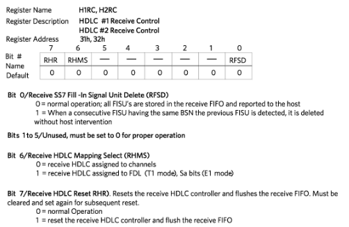
| 31 | H1RC | HDLC #1 Receive Control | Information available in HDLC section | |
| 32 | H2RC | HDLC #2 Receive Control | Unsupported function in the DS26401 | |
| 33 | E1RCR1 | E1 Receive Control Register 1 | 0 = RCR1.0 1 = RCR1.1 2 = RCR1.2 3 = RCR1.3 4 = RCR1.4 5 = RCR1.6 6 = RCR1.5 7 = RCR3.5 |
|
| 34 | E1RCR2 | E1 Receive Control Register 2 | 0 = RCR2.0 1 = 2 = NS * 3 = NS * 4 = NS * 5 = NS * 6 = NS * 7 = NS * |
* The RLINK and RLCLK functions are not supported on the DS26401 |
| 35 | E1RCR1 | E1 Transmit Control Register 1 | 0 = TCR1.0 1 = TCR1.5 2 = TCR1.2 3 = TCR1.3 4 = TCR1.4 5 = TCR1.1 6 = TCR1.6 7 = TCR1.7 |
|
| 36 | E1TCR2 | E1 Transmit Control Register 2 | 0 = TCR2.5 1 = TCR2.6 2 = TCR2.7 3 = NS * 4 = NS * 5 = NS * 6 = NS * 7 = NS * | * The TLINK and TLCLK functions are not supported on the DS26401 |
| 37 | BOCC | BOC Control Register | 0 = THC2.6 1 = RBOCC.1 2 = RBOCC.2 3 = RBOCC.7 4 = NS * 5 = 6 = 7 = | * The DS26401 has a dedicated receieve BOC message register |
| 40 | SIGCR | Signaling Control Register | 0 = RFSA1.4 * 1 = 2 = 3 = RSIGC.2 4 = RSIGC.1 5 = 6 = 7 = NS ** | * The DS26401 forces signaling to all ones on a per channel basis using the RSAOI1 - RSAOI4 registers ** THe DS26401 selects signaling re-insertion on a per channel basis using the SRI1 - SRI4 registers |
| 41 | ERCNT | Error Count Configuration Register | 0 = ERCNT.0 * 1 = ERCNT.1 2 = ERCNT.2 3 = ERCNT.0 4 = ERCNT.3 5 = ERCNT.4 6 = ERCNT.5 7 = - | * T1 Mode ** E1 Mode |
| 4A | LBCR | Loopback Control Register | 0 = RCR3.0 1 = RCR3.1 2 = RCR3.2 3 = NS * 4 = NS * 5 = - 6 = - 7 = - | * LIU functions are not supported |
| 4F | ESCR | Elastic Store Control Register | 0 = RESCR.0 1 = RESCR.1 2 = RESCR.2 3 = RESCR.3 4 = TESCR.0 5 = TESCR.1 6 = TESCR.2 7 = TESCR.3 | |
| 70 | CCR1 | Common Control Register 1 | 0 = TCR3.3 1 = TCR3.4 2 = TCR3.5 3 = NS * 4 = TCR3.6 5 = RSIGC.0 6 = TCR3.0 7 = NS * | * The DS26401 does not use Indirect Registers ** LIU functions are not supported |
| 71 | CCR2 | Common Control Register 2 | 0 = NS * 1 = GCR2.4 2 = GCR2.5 3 = 4 = 5 = 6 = 7 = | |
| 72 | CCR3 | Common Control Register 3 | 0 = RESCR.6 1 = RESCR.7 2 = TESCR.6 3 = TESCR.7 4 = 5 = 6 = GCR1.0 7 = NS * | * Unsupported function in the DS26401 |
| 73 | CCR4 | Common Control Register 4 | 0 = NS * 1 = NS * 2 = NS * 3 = NS * 4 = NS ** 5 = NS ** 6 = NS ** 7 = NS ** | * The DS26401 does not have user definable output pins ** LIU functions are not supported |
| 78 | LIC1 | Line Interface Control 1 | Unsupported function in the DS26401 | |
| 79 | LIC2 | Line Interface Control 2 | Unsupported function in the DS26401 | |
| 7A | LIC3 | Line Interface Control 3 | Unsupported function in the DS26401 | |
| 7B | LIC4 | Line Interface Control 4 | Unsupported function in the DS26401 | |
| 7C | UNUSED | |||
| 7D | TLBC | Transmit Line Build-Out Control | Unsupported function in the DS26401 | |
| 7E | IAAR | Idle Array Address Register | The DS26401 does not use Direct Registers | |
| 7F | PCICR | Per-Channel Idle Code Value Register | The DS26401 does not use Direct Registers | |
| 90-9F | HDLC1 | HDLC #1 Functions Registers | Information available in HDLC section | |
| A0-AF | HDLC2 | HDLC#2 Functions Registers | Unsupported function in the DS26401 | |
| B0 | ESIBCR1 | Extended System Information Bus Control Register 1 | Unsupported function in the DS26401 | |
| B1 | ESIBCR2 | Extended System Information Bus Control Register 2 | Unsupported function in the DS26401 | |
| B2 | ESIB1 | Extended System Information Bus Register 1 | Unsupported function in the DS26401 | |
| B3 | ESIB2 | Extended System Information Bus Control Register 1 | Unsupported function in the DS26401 | |
| B4 | ESIB3 | Extended System Information Bus Register 3 | Unsupported function in the DS26401 | |
| B5 | ESIB4 | Extended System Information Bus Register 4 | Unsupported function in the DS26401 | |
| B6 | IBCC | In-Band Code Control Register | 0 = RIBCC.0 1 = RIBCC.1 2 = RIBCC.2 3 = RIBCC.3 4 = RIBCC.4 5 = RIBCC.5 6 = TCR4.0 7 = TCR4.1 |
|
| BD | RSCC | In-Band Receive Spare Control Register | 0 = RSCC.0 1 = RSCC.1 2 = RSCC.2 3 = 4 = 5 = 6 = 7 = |
|
| C2 | RFDLM1 | Receive FDL Match Register 1 | Unsupported Function in the DS26401 | |
| C3 | RFDLM2 | Receive FDL Match Register 2 | Unsupported Function in the DS26401 | |
| C4 | Unused | Unused | ||
| C5 | IBOC | Interleave Bus Operation Control Register | The DS26401 Interleave Bus Operation function has separate receive and transmit control registers | |
| ||||
| DB-E1 | BERT | BERT Functions Registers | Information available in BERT section | |
| E2 | Unused | Unused | ||
| E3-EF | BERT | BERT Functions Registers | Information available in BERT section | |
| F0-FF | TEST | Test Register | Unsupported function in the DS26401 | |
HDLC Controller
The DS26401 has a single HDLC controller that may be mapped to any time slot or to the FDL (T1 mode) or any combinations of Sa bits (E1 mode). The table below list the differences between the DS2155's and the DS26401's HDLC function.| FUNCTION | DS2155 | DS26401 |
| Number of Controllers | 2 | 1 |
| FIFO Size | 128 bytes | 64 bytes |
| Channel Assignment | Any combination of channels; Facilities Data Link bit stream; Any combination of Sa bits |
Any single DS0; Facilities Data Link bit stream; Any combination of Sa bits |
| SS7 Support | Yes | No |
| DS2155 | DS26401 BIT LOCATION; 2155 BIT = 26401 REG. BIT |
COMMENTS | ||
| ADDRESS | NAME | FUNCTION | ||
| 31 | H1RC | HDLC #1 Receive Control | 0 = NS * 1 = 2 = 3 = 4 = 5 = 6 = RHC1.5 7 = RHC1.6 |
* The DS26401 does not have support for Signaling System 7 (SS7) |
| 32 | H2RC | HDLC #2 Receive Control | Unsupported function in the DS26401 | |
| 90 | H2RC | HDLC #2 Receive Control | 0 = THC1.0 1 = THC1.1 2 = THC1.2 3 = THC1.3 4 = THC1.4 5 = THC1.5 6 = THC1.6 7 = THC1.7 |
|
| 91 | H1FC | HDLC #1 FIFO Control | 0 = RHFC.0 1 = RHFC.1 2 = NS * 3 = THFC.0 4 = THFC.1 5 = NS * 6 = 7 = |
* The HDLC FIFO is only 64 bytes deep on the DS26401 |
| 92 | H1RCS1 | HDLC #1 Receive Channel Select 1 | The DS26401 uses the RHC register to select the channel to receive HDLC data The DS26401 can only receive HDLC data in a single DSO channel | |
| 93 | H1RCS2 | HDLC #2 Receive Channel Select 2 | ||
| 94 | H1RCS3 | HDLC #2 Receive Channel Select 3 | ||
| 95 | H1RCS4 | HDLC #2 Receive Channel Select 4 | ||
| 96 | H1RTSBS | HDLC #1 Receive Time Slot Bits/Sa Bits Select | ||
| 97 | H1TCS1 | HDLC #1 Transmit Channel Select 1 | The DS26401 uses the THC2 register to select the channel to transmit HDLC data The DS26401 can only transmit HDLC data in a single DSO channel | |
| 98 | H1TCS2 | HDLC #1 Transmit Channel Select 2 | ||
| 99 | H1TCS3 | HDLC #1 Transmit Channel Select 3 | ||
| 9A | H1TCS4 | HDLC #1 Transmit Channel Select 4 | ||
| 9B | H1TTSBS | HDLC #1 Transmit Time Slot Bits/Sa Bits Select | ||
| 9C | H1RPBA | HDLC #1 Receive Packet Bytes Available | 0B5 RHPBA |
|
| 9D | H1TF | HDLC #1 Transmit FIFO | 1B4 THF |
|
| 9E | H1RF | HDLC #1 Receive FIFO | 0B6 RHF |
|
| 9F | H1TFBA | HDLC #1 Transmit FIFO Buffer Available | 1B3 TFBA |
|
| A0 | H2TC | HDLC #2 Transmit Control | Unsupported function in the DS26401 | |
| A1 | H2FC | HDLC #2 FIFO Control | Unsupported function in the DS26401 | |
| A2 | H2RCS1 | HDLC #2 Receive Channel Select 1 | Unsupported function in the DS26401 | |
| A3 | H2RCS2 | HDLC #2 Receive Channel Select 2 | Unsupported function in the DS26401 | |
| A4 | H2RCS3 | HDLC #2 Receive Channel Select 3 | Unsupported function in the DS26401 | |
| A5 | H2RCS4 | HDLC #2 Receive Channel Select 3 | Unsupported function in the DS26401 | |
| A6 | H2RTSBS | HDLC #2 Receive Time Slot Bits/Sa Bits Select | Unsupported function in the DS26401 | |
| A7 | H2TCS1 | HDLC #2 Transmit Channel Select 1 | Unsupported function in the DS26401 | |
| A8 | H2TCS2 | HDLC #2 Transmit Channel Select 2 | Unsupported function in the DS26401 | |
| A9 | H2TCS3 | HDLC #2 Transmit Channel Select 3 | Unsupported function in the DS26401 | |
| AA | H2TCS4 | HDLC #2 Transmit Channel Select 4 | Unsupported function in the DS26401 | |
| AB | H2TTSBS | HDLC #2 Transmit Time Slot Bits/Sa Bits Select | Unsupported function in the DS26401 | |
| AC | H2RPBA | HDLC #2 Receive Packet bytes Available | Unsupported function in the DS26401 | |
| AD | H2TF | HDLC #2 Transmit FIFO | Unsupported function in the DS26401 | |
| AE | H2RF | HDLC #2 Receive FIFO | Unsupported function in the DS26401 | |
| AF | H2TFBA | HDLC #2 Transmit FIFO Buffer Available | Unsupported function in the DS26401 | |
BERT Functions
The DS26401 BERT functions are more full featured than the DS2155, therefore a direct register mapping is not possible. The DS26401 pseudorandom patterns are fully programmable over 32 bits compared to the fixed set of pseudorandom patterns found in the DS2155. Also, large repetitive patterns up to 512 bytes may be loaded via an indirect register. The BERT register set for the DS2155 is below but the DS26401 data sheet should be consulted for all BERT functions.| DS2155 | COMMENTS | ||
| ADDRESS | NAME | FUNCTION | |
| DB | BAWC | BERT Alternating Word Count Rate | Consult DS26401 Data Sheet |
| DC | BRP1 | BERT Repetitive Pattern Set Register 1 | Consult DS26401 Data Sheet |
| DD | BRP2 | BERT Repetitive Pattern Set Register 2 | Consult DS26401 Data Sheet |
| DE | BRP3 | BERT Repetitive Pattern Set Register 3 | Consult DS26401 Data Sheet |
| DF | BRP4 | BERT Repetitive Pattern Set Register 4 | Consult DS26401 Data Sheet |
| E0 | BC1 | BERT Control Register 1 | Consult DS26401 Data Sheet |
| E1 | BC2 | BERT Control Register 2 | Consult DS26401 Data Sheet |
| E2 | -- | Unused | Unused |
| E3 | BBC1 | BERT Bit Count Register 1 | Consult DS26401 Data Sheet |
| E4 | BBC2 | BERT Bit Count Register 2 | Consult DS26401 Data Sheet |
| E5 | BBC3 | BERT Bit Count Register 3 | Consult DS26401 Data Sheet |
| E6 | BBC4 | BERT Bit Count Register 4 | Consult DS26401 Data Sheet |
| E7 | BEC1 | BERT Error Count Register 1 | Consult DS26401 Data Sheet |
| E8 | BEC2 | BERT Error Count Register 2 | Consult DS26401 Data Sheet |
| E9 | BEC3 | BERT Error Count Register 3 | Consult DS26401 Data Sheet |
| EA | BIC | BERT Interface Control Register | Consult DS26401 Data Sheet |
| EB | ERC | Error Rate Control Register | Consult DS26401 Data Sheet |
| EC | NOE1 | Number-of-Errors 1 | Consult DS26401 Data Sheet |
| ED | NOE2 | Number-of-Errors 3 | Consult DS26401 Data Sheet |
| EE | NOEL1 | Number-of-Errors Left 1 | Consult DS26401 Data Sheet |
| EF | NOEL2 | Number-of-Errors Left 2 | Consult DS26401 Data Sheet |
Featured Exclusive to the DS26401
The DS26401 has many new features, which are summarized below.Transmit-Side Synchronizer
The DS26401 has a basic synchronizer on the transmit side. This function allows the transmitter to align to the data stream present at TSER when there is no externally supplied frame sync signal available.TSYNCC.0: Resynchronize (RESYNC). When toggled from low to high, a resynchronization of the transmit side framer is initiated. Must be cleared and set again for a subsequent resync.
TSYNCC.1: Sync Enable (SYNCE)
0 = Automatic resync enabled
1 = Automatic resync disabled
TSYNCC.2: Transmit Synchronizer Enable (TSEN)
0 = Transmit-Side Synchronizer Disabled
1 = Transmit-Side Synchronizer Enabled
TLS3.0: Loss-of-Frame Synchronization Detect (LOFD). This is a latched bit which is set when the transmit synchronizer is searching for the sync pattern in the incoming data stream.
TLS3.1: Loss of Frame (LOF). A real-time status bit which indicates that the transmit side synchronizer is searching for the synchronization pattern in the incoming data stream.
Other Functions Exclusive to the DS26401
A low-to-high transition on this bit latches the framer performance monitor counters, and the internal BERT counters (only when enabled). Each framer as well as the BERT can be independently enabled to accept this input. Must be cleared and set again to perform another counter latch.GCR1.2: Bulk Write Enable (BWE). When this bit is set, a port write to one of the octal ports will be mapped into all eight ports. Useful for device initialization.
0 = Normal operation
1 = Bulk write is enabled
GCR1.3: Reference Clock Frequency Select (REFCLKS). This bit sets the divider ratio of the internal clock generator depending on the frequency of the reference clock input.
0 = REF_CLK is 1.544MHz
1 = REF_CLK is 2.048MHz
GCR1.4: Ganged IBO Enable (GIBO). This bit is used to select either the internal MUX for IBO operation or externally "wire-or" operation. Normally this bit should be set = 0 and the internal MUX used.
0 = Use internal IBO mux.
1 = Externally "wire-or" TSER pins and RSER pins for IBO operation.
GCR1.5: Receive Loss-of-Frame/Loss-of-Transmit Clock indication Select (RLOFLTS)
0 = RLOF/LOTCx pins indicate receive loss of frame
1 = RLOF/LOTCx pins indicate loss of transmit clock
GCR1.6: BERT Loss-of-Sync Interrupt Mask (BLOSIM)
0 = DS26401 will not generate an interrupt on INT for a BERT LOS
1 = DS26401 will generate an interrupt on INT for a BERT LOS
GCR1.7: BERT Bit Error Detect Interrupt Mask (BBEDIM)
0 = DS26401 will not generate an interrupt on INT for a BERT bit error detect
1 = DS26401 will generate an interrupt on INT for a BERT bit error detect
GCR2. 0: Receive Channel Block/Clock Select (RCBCS)
This bit controls the function of all eight RCHBLK/CLK pins.
0 = RCHBLK/CLK pins output RCHBLK(1-8) (Receive Channel Block)
1 = RCHBLK/CLK pins output RCHCLK(1-8) (Receive Channel Clock)
GCR2.1: Transmit Channel Block/Clock Select (TCBCS).
This bit controls the function of all eight TCHBLK/CLK pins.
0 = TCHBLK/CLK pins output TCHBLK(1-8) (Transmit Channel Block)
1 = TCHBLK/CLK pins output TCHCLK(1-8) (Transmit Channel Clock)
GCR2.2: Receive Frame/Multiframe Sync Select (RFMSS).
This bit controls the function of all eight RF/RMSYNC pins.
0 = RF/RMSYNC pins output RFSYNC(1-8) (Receive Frame Sync)
1 = RF/RMSYNC pins output RMSYNC(1-8) (Receive Multiframe Sync)
GCR2.3: Receive Loss-of-Signal/Signaling Freeze Select (RLOSSFS). This bit controls the function of all eight RLOS/RSIGF pins.
0 = RLOS/RSIGF pins output RLOS(1-8) (receive loss of signal)
1 = RLOS/RSIGF pins output RSIGF(1-8) (receive signaling freeze)
GCR2.6 and GCR2.7: Interleave Bus Operation Mode Select 0-1 (IBOMS0/1). These bits determine the configuration of the IBO (interleaved bus) multiplexer. These bits should be with the Rx and Tx IBO control registers within each of the framer units. Additional information concerning the IBO mux is given in the data sheet.
| IBOMS1 | IBOMS0 | IBO Mode |
| 0 | 0 | IBO Mux Disabled |
| 0 | 1 | 4.096MHz (2 per) |
| 1 | 0 | 8.192MHz (4 per) |
| 1 | 1 | 16.384MHz (8 per) |
RCR.1: Receive RAI Integration Enable (RAIIE). In T1 ESF mode, the RAI indication can be interrupted for a period not to exceed 100ms per interruption as stated in ANSI T1.403. In T1 ESF mode, setting RAIIE will cause the RAI status from the DS26401 to be integrated for 200ms.
0 = RAI detects when 16 consecutive patterns of 00FF appear in the FDL. RAI clears when 14 or less patterns of 00FF hex out of 16 possible appear in the FDL
1 = RAI detects when the condition has been present for greater than 200ms. RAI clears when the condition has been absent for greater than 200ms.
RCR3.7: Input Data Format (IDF)
0 = Bipolar data is expected at RPOS and RNEG (either AMI or B8ZS)
1 = NRZ data is expected at RPOS. The BPV counter will be disabled and RNEG will be ignored by the DS26401.
RRTS1.0: Receive Loss-of-Frame Condition (RLOF). Set when the DS26401 is not synchronized to the received data stream.
RRTS1.1: Receive Loss-of-Signal Condition (RLOS). Set when 255 (or 2048 if RCR2.0 = 1) consecutive zeros have been detected at RPOS and RNEG.
RRTS1.2: Receive Alarm Indication Signal Condition (RAIS). Set when an unframed all one's code is received at RPOS and RNEG.
RRTS1.3: Receive Remote Alarm Indication Condition (RRAI). Set when a remote alarm is received at RPOS and RNEG.
RRTS3.0:(T1 MODE) Loop-Up Code Detected Condition (LUP). Set when the loop-up code as defined in the RUPCD1/2 register is being received.
RRTS3.0:(E1 MODE) Receive Distant MF Alarm Condition (RDMA). Set when bit-6 of time slot 16 in frame 0 has been set for two consecutive multiframes. This alarm is not disabled in the CCS signaling mode.
RRTS3.1:(T1 MODE) Loop-Down Code Detected Condition (LDN). Set when the loop-down code as defined in the RDNCD1/2 register is being received.
RRTS3.1: (E1 MODE) V5.2 Link Detected Condition (V52LNK). Set on detection of a V5.2 link identification signal (G.965).
RRTS3.2: Spare Code Detected Condition (LSP). Set when the spare code as defined in the RSCD1/2 registers is being received.
RRTS3.3: Loss-of-Receive Clock Condition (LORC). Set when the RCLK pin has not transitioned for one channel time.
RLS4.2: One-Second Timer (1SEC). Set every one-second interval based on RCLK.
RLS7.3: Receive SLC-96 Alignment Event (RSLC96). Set when a valid SLC-96 alignment pattern is detected in the Fs bit stream, and the RSLCx registers have data available for retrieval. (Section 11.12)
RLS7.5: Receive RAI-CI Detect (RRAI-CI). Set when an RAI-CI pattern has been detected by the receiver (see Section 11.5.1). This bit is active in ESF framing mode only, and will set only if an RAI condition is being detected (RRTS1.3). When the host reads (and clears) this bit, it will set again each time the RAI-CI pattern is detected (approximately every 1.1 seconds).
ERCNT.6: Manual Counter Update Select (MCUS). When manual update mode is enabled with EAMS, this bit can be used to allow the GLCE bit in GCR1 to latch all counters. Useful for synchronously latching counters of multiple framers.
0 = MECU is used to manually latch counters.
1 = GLCE is used to manually latch counters.
ERCNT.7: One-Second Select (1SECS). When timed update is enabled by EAMS, setting this bit for a specific framer will allow that framer's counters to latch on the 1 second reference from framer #1. Note that this bit should always be clear for framer #1.
0 = Use internally generated 1 second timer.
1 = Use 1 second timer from framer #1.
RESCR.4: Receive Slip Zone Select (RSZS). This bit determines the minimum distance allowed between the elastic store read and write pointers before forcing a controlled slip. This bit is only applies during T1 to E1 or E1 to T1 conversion applications.
0 = force a slip at 9 bytes or less of separation (used for clustered blank channels)
1 = force a slip at 2 bytes or less of separation (used for distributed blank channels)
RBOCC.4 to RBOCC.5: Receive BOC Disintegration bits (RBD0, RBD1). The BOC Disintegration filter sets the number of message bits that must be received without a valid BOC in order to set the BC bit indicating that a valid BOC is no longer being received.
| RBD1 | RBD0 | CONSECUTIVE MESSAGE BITS FOR BOC CLEAR IDENTIFICATION |
| 0 | 0 | 16 |
| 0 | 1 | 32 |
| 1 | 0 | 48 |
| 1 | 1 | 64 |
TCR3.1: Insert BPV (IBPV). A 0-to-1 transition on this bit will cause a single bipolar violation (BPV) to be inserted into the transmit data stream. Once this bit has been toggled from a 0 to a 1, the device waits for the next occurrence of three consecutive ones to insert the BPV. This bit must be cleared and set again for a subsequent error to be inserted.
TIOCR.3: TSSYNC Mode Select (TSSM). Selects frame or multiframe mode for the TSSYNC pin.
0 = frame mode
1 = multiframe mode
TLS1.4: Transmit SLC96 Multiframe Event (TSLC96). When enabled by TCR2.6, this bit will set once per SLC96 multiframe (72 frames) to alert the host that new data may be written to the TSLC1-TSLC3 registers.
TESCR.4: Transmit Slip Zone Select (TSZS). This bit determines the minimum distance allowed between the elastic store read and write pointers before forcing a controlled slip. This bit only affects the elastic stores when used in T1 to E1 or E1 to T1 conversion applications.
0 = force a slip at 9 bytes or less of separation (used for clustered blank channels)
1 = force a slip at 2 bytes or less of separation (used for distributed blank channels)
 電子發燒友App









評論