Abstract: Design idea outlining how to use an I2C-controlled analog switch to triple the number of devices connected to an I2C bus.
Perhaps the most effective way to gain board space and increase component density is to minimize wiring on the board. A widely used architecture that allows such miniaturization is the I2C bus. Comprising only a bidirectional data line, SDA, and a clock line, SCL, this bus requires no chip selects or other additional connections.
Microcontrollers from Philips, Microchip, and other manufacturers include dedicated I2C interfaces, but you can also implement the interface in software. To complete this task, you associate a 7-bit address with each master or slave transceiver and factory- or pin-program the device with two to four address options.
An increasing number of slaves now include the I2C interface, but some of their 128 address locations are reserved for special functions, so not all locations are available to a designer. Yet, two or more devices could have the same address in some applications.
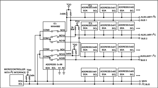
In Figure 1, analog switch IC1, which is I2C-controlled, connects auxiliary branches that contain devices with the same address to the main I2C bus. IC2 and IC3, for example, have the same address but are located on different auxiliary buses.

Figure 1. This I2C-controlled analog switch expands by three the number of devices connected to the bus.
The arrangement in Figure 1 prevents the master from addressing multiple slaves at the same time. If that situation occurs, the data becomes corrupted during a master-read protocol, and all slaves may not receive data during a master-write protocol. The analog switch accepts bidirectional signals as required for the SDA line. The switch has low on-state resistance, adds almost no leakage on the lines, and provides four selectable slave addresses. You simultaneously control the switches by using the simple SendByte protocol (address plus 8-bit command).
You can switch the three auxiliary buses on the fly. Power-up sets the switches to soft mode, an off state with 12-msec switching time. Then, a command byte of 0b11000000 sets the switches to hard mode (400-nsec switching time). Subsequent commands select the desired auxiliary bus. Command 0b1000011, for example, selects auxiliary bus 1.
The main I2C bus includes necessary pullup resistors, and the auxiliary buses include weaker pullups that ensure a high state when you deselect the bus. The circuit in Figure 1 allows you to add three times more devices on the bus. For a wider selection, you can replace the MAX4562 with a MAX4572, whose 14 switches allow you to add as many as seven auxiliary buses.
A similar version of this article appeared in the November 22, 2001 issue of EDN magazine.
Perhaps the most effective way to gain board space and increase component density is to minimize wiring on the board. A widely used architecture that allows such miniaturization is the I2C bus. Comprising only a bidirectional data line, SDA, and a clock line, SCL, this bus requires no chip selects or other additional connections.
Microcontrollers from Philips, Microchip, and other manufacturers include dedicated I2C interfaces, but you can also implement the interface in software. To complete this task, you associate a 7-bit address with each master or slave transceiver and factory- or pin-program the device with two to four address options.
An increasing number of slaves now include the I2C interface, but some of their 128 address locations are reserved for special functions, so not all locations are available to a designer. Yet, two or more devices could have the same address in some applications.
In Figure 1, analog switch IC1, which is I2C-controlled, connects auxiliary branches that contain devices with the same address to the main I2C bus. IC2 and IC3, for example, have the same address but are located on different auxiliary buses.

Figure 1. This I2C-controlled analog switch expands by three the number of devices connected to the bus.
The arrangement in Figure 1 prevents the master from addressing multiple slaves at the same time. If that situation occurs, the data becomes corrupted during a master-read protocol, and all slaves may not receive data during a master-write protocol. The analog switch accepts bidirectional signals as required for the SDA line. The switch has low on-state resistance, adds almost no leakage on the lines, and provides four selectable slave addresses. You simultaneously control the switches by using the simple SendByte protocol (address plus 8-bit command).
You can switch the three auxiliary buses on the fly. Power-up sets the switches to soft mode, an off state with 12-msec switching time. Then, a command byte of 0b11000000 sets the switches to hard mode (400-nsec switching time). Subsequent commands select the desired auxiliary bus. Command 0b1000011, for example, selects auxiliary bus 1.
The main I2C bus includes necessary pullup resistors, and the auxiliary buses include weaker pullups that ensure a high state when you deselect the bus. The circuit in Figure 1 allows you to add three times more devices on the bus. For a wider selection, you can replace the MAX4562 with a MAX4572, whose 14 switches allow you to add as many as seven auxiliary buses.
A similar version of this article appeared in the November 22, 2001 issue of EDN magazine.
 電子發燒友App







評論