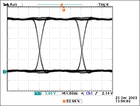
Abstract: A handful of components are integrated into a circuit that creates a high-quality random data stream that generates eye diagrams up to 62.5MHz. The circuit diagram and eye diagram are shown.
The eye diagram, one of the best figures of merit for evaluating robustness in a digital data link, shows a single bit window (bit N), preceded by a random-value bit (N-1) and followed by a random-value bit (N+1).
Communications-systems engineers usually have access to the sophisticated test equipment required to measure and analyze the bit-error rate for a communications channel, but most other engineers do not. For the latter group, the circuit of Figure 1 provides an alternative—a stimulus derived from a single digital source.
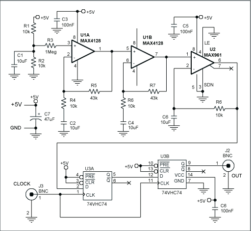
Figure 1. A handful of components creates a high-quality random data stream for generating eye diagrams.
Resistors R1 and R2 set up a bias of VCC/2, which is bypassed to ground by C1. A large 1MΩ resistor (R3) serves as a small-signal wideband noise source. Amplifiers U1A and U1B each provide an AC gain of 5V/V, but at low frequencies their gain is unity due to capacitors C2 and C4. The amplified noise at the output of U1B drives comparator U2, which outputs a digital signal suitable for input to the D-type flip-flops (U3A and U3B).
The comparator's output is fed back to its inverting input through a lowpass filter, forcing a near-50% duty cycle at the output. As a result, U3A's output is a data stream of random bit values that are synchronous with the circuit's clock input. Unfortunately, the comparator-output signal frequently violates U3A's setup and hold times, causing too much jitter at the output of U3A. That problem is corrected by clocking the resulting data stream through a second D flip-flop (U3B).
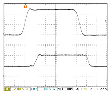
The circuit with components as shown works up to 62.5Mbps (see the eye diagram of Figure 2). At 20Mbps it exhibits less than 200psP-P jitter, making it suitable for common protocols such as RS-422, RS-485, CAN, USB, RS-232, and PROFIBUS.

Figure 2. An eye diagram from the Figure 1 output shows that the 20Mbps circuit functions up to 62.5Mbps.
The choice of amplifier, comparator, and flip-flop depends on the intended application. Amplifiers U1A and U1B should have a bandwidth comparable to the maximum desired output frequency (in this case, a MAX4128 with gain-bandwidth product of 25MHz). This op amp specifies stability for gains of 10 or more. For the present application, stability is not a primary concern.
To provide a reasonable amount of random data, the comparator's propagation delay should be comparable to the shortest desired bit period (too much propagation delay could eliminate one of the possible states between bits N-1, N, and N+1). The MAX961 with its 4.5ns propagation delay is a good choice. The flip-flops should provide a clean edge with fast rise times and little or no overshoot. A 74VHC74 was selected to match the 2.7V to 5.5V range of the amplifiers and comparator. The 74VHC74 operates from 2V to 5.5V, with a minimum switching frequency (at 3V supply) of 80MHz. To use the circuit, connect a power supply (VCC) of 2.7V to 5.5V, and a clock source. For best operation the clock source should be terminated with 50Ω, and have a full swing from ground to VCC. Connect the output through a short piece of coax to the input of the device under test (DUT). Do not terminate this line, because the flip-flop output cannot drive 50Ω loads. Because the flip-flops divide the clock frequency by two, use the desired bit frequency as the clock frequency (i.e., for 10Mbps, set the clock to 10MHz). Connect the DUT output to an oscilloscope with sufficient bandwidth, trigger the scope from the clock source, and set the scope's persistence to infinity.
A similar version of this article appeared in the November 15, 2004 issue of EE Times, Planet Analog Supplement magazine.
The eye diagram, one of the best figures of merit for evaluating robustness in a digital data link, shows a single bit window (bit N), preceded by a random-value bit (N-1) and followed by a random-value bit (N+1).
Communications-systems engineers usually have access to the sophisticated test equipment required to measure and analyze the bit-error rate for a communications channel, but most other engineers do not. For the latter group, the circuit of Figure 1 provides an alternative—a stimulus derived from a single digital source.

Figure 1. A handful of components creates a high-quality random data stream for generating eye diagrams.
Resistors R1 and R2 set up a bias of VCC/2, which is bypassed to ground by C1. A large 1MΩ resistor (R3) serves as a small-signal wideband noise source. Amplifiers U1A and U1B each provide an AC gain of 5V/V, but at low frequencies their gain is unity due to capacitors C2 and C4. The amplified noise at the output of U1B drives comparator U2, which outputs a digital signal suitable for input to the D-type flip-flops (U3A and U3B).
The comparator's output is fed back to its inverting input through a lowpass filter, forcing a near-50% duty cycle at the output. As a result, U3A's output is a data stream of random bit values that are synchronous with the circuit's clock input. Unfortunately, the comparator-output signal frequently violates U3A's setup and hold times, causing too much jitter at the output of U3A. That problem is corrected by clocking the resulting data stream through a second D flip-flop (U3B).
The circuit with components as shown works up to 62.5Mbps (see the eye diagram of Figure 2). At 20Mbps it exhibits less than 200psP-P jitter, making it suitable for common protocols such as RS-422, RS-485, CAN, USB, RS-232, and PROFIBUS.

Figure 2. An eye diagram from the Figure 1 output shows that the 20Mbps circuit functions up to 62.5Mbps.
The choice of amplifier, comparator, and flip-flop depends on the intended application. Amplifiers U1A and U1B should have a bandwidth comparable to the maximum desired output frequency (in this case, a MAX4128 with gain-bandwidth product of 25MHz). This op amp specifies stability for gains of 10 or more. For the present application, stability is not a primary concern.
To provide a reasonable amount of random data, the comparator's propagation delay should be comparable to the shortest desired bit period (too much propagation delay could eliminate one of the possible states between bits N-1, N, and N+1). The MAX961 with its 4.5ns propagation delay is a good choice. The flip-flops should provide a clean edge with fast rise times and little or no overshoot. A 74VHC74 was selected to match the 2.7V to 5.5V range of the amplifiers and comparator. The 74VHC74 operates from 2V to 5.5V, with a minimum switching frequency (at 3V supply) of 80MHz. To use the circuit, connect a power supply (VCC) of 2.7V to 5.5V, and a clock source. For best operation the clock source should be terminated with 50Ω, and have a full swing from ground to VCC. Connect the output through a short piece of coax to the input of the device under test (DUT). Do not terminate this line, because the flip-flop output cannot drive 50Ω loads. Because the flip-flops divide the clock frequency by two, use the desired bit frequency as the clock frequency (i.e., for 10Mbps, set the clock to 10MHz). Connect the DUT output to an oscilloscope with sufficient bandwidth, trigger the scope from the clock source, and set the scope's persistence to infinity.
A similar version of this article appeared in the November 15, 2004 issue of EE Times, Planet Analog Supplement magazine.
 電子發燒友App










評論