Abstract: This application note addresses the Dallas Semiconductor DS80C320 high-speed microcontroller when used with external program memory. Due to the high speed of this device, critical memory interface timing constraints are examined. This application note discusses the DS80C320, but is applicable to all Dallas Semiconductor Microcontrollers.
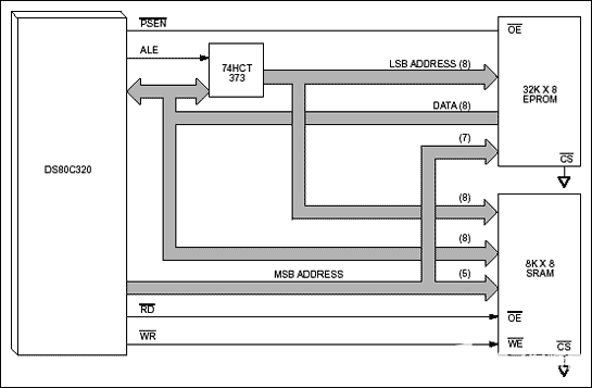
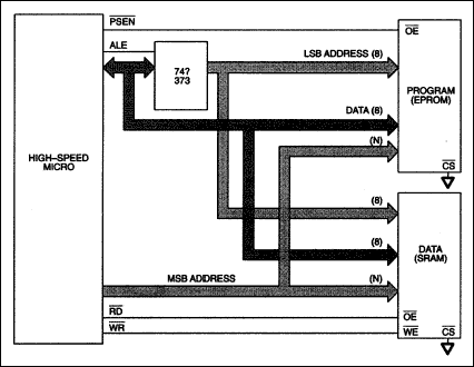
A typical configuration for a DS80C320 processor system is shown in Figure 1. A 32K x 8 EPROM is used to hold program information, and a 8K x 8 Static RAM is used for data storage. The Least Significant Byte (LSB) of the memories' address is time multiplexed with data on processor pins AD7 through AD0. The signal ALE from the processor goes high before a new address is placed on the bus and goes low before it is removed. In Figure 1, the action of ALE going low is used to latch the address into a 74HCT373 8-bit transparent latch. The 74HCT373 then provides its latched address output to the memories while the AD7 through AD0 CPU bus carries data. The MSB of the address is not multiplexed, and is available on port pins P2.7 through P2.0 (A15-A9).
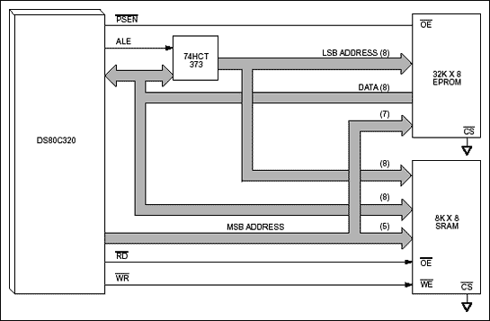
Figure 1. A typical DS80C320 system confirguration.
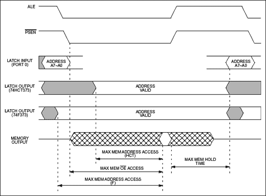
Figure 2. Program memory interface timing.
While EPROM devices with access times of 26 ns or less may be available, they are likely to be expensive. A simple and more cost effective approach to solving this timing constraint is to use a faster latch technology; an 74F373 for instance. Using the same analysis as above, if the propagation delay of the F373 latch, 8 ns, is subtracted from the tAVIV1 parameter (64 ns) you arrive at an address access requirement of 56 ns. This is much easier to realize than 26 ns.
There is another timing constraint that suggests the use of an "F" type part in faster applications. On a 74HCT373 latch, the minimum required hold time of the input after the latch enable (ALE) goes low may be as much as 13 ns. The latch's input, the address out of the processor, is held until it is driven by the memory's output. This output is enabled by active-low PSEN. Again referring to the data sheet, it can be seen that active-low PSEN may occur as quickly as 0.5 ns after ALE falls (parameter tLLPL). If the memory's output begins to drive the bus immediately after active-low PSEN enables it, then there may only be 0.5 ns hold time. That obviously violates the latch's requirement. While it is reasonable to assume that there will be some delay before the memory's output will drive the bus, this is not a specified (or tested) parameter. Therefore a conservative estimate of 5 ns will be assumed. From above numbers and the equation for the tLLPL parameter (0.25tCLCL-7), it can be calculated that clock frequencies of 19.23 MHz and below will allow sufficient hold time to satisfy the 74HCT373 latch's requirement. Note that the hold time for a 74F373 latch is 3 ns which is met under all conditions.
From the above analysis, you could choose 19.32 MHz as the latch technology switchover point, however, there is a reason why this was not done. Referring back to the address access equation (3tCLCL-24), it can be calculated that if a 74HCT373 latch is used for frequencies higher than 16.31 MHz, then a 90 ns or faster memory device is required. Therefore as a trade-off between latch speed and EPROM speed, the 74F373 latch (less expensive than a fast EPROM) is recommended for crystal frequencies greater than or equal to 16.31 MHz, and the 74HCT373 for lower frequencies.
As shown in Figure 1, active-low PSEN enables the EPROM's output, so the timing for this signal must also be considered when choosing a device. The DS80C320 data sheet specifies the time from active-low PSEN low to a valid instruction in must be no more than 70 ns (parameter tPLIV). This is therefore the maximum allowed access time from the memory's active-low OE pin. In summary, the two timing requirements for the selected EPROM are that the address access time must be less than 92 ns and the active-low OE access time must be less than 70 ns. When looking at EPROM data sheets, it can be seen that common access time combinations (address access, active-low OE access) are 55,35; 70,40; 90,40; 120,50; 150,65; 200,75; and 250,100 ns. The 55, 35 device meets both timing requirements for a 33 MHz clock on the DS80C320 and is the recommended selection.
Table 1 shows the slowest EPROM memory speeds recommended for various processor clock frequencies. If for some reason it is desirable to use devices faster than those recommended, this is possible. For this document, the memory speeds available (maximum access times from address and active-low OE respectively) are assumed to be those indicated above, however, any combination that meets the two requirements may be used. In Table 1, the memory speeds shown in bold are the recommended configurations.
Table 1. Recommended EPROM speeds
It should be noted that it is often possible to reduce the power consumption of EPROMs by keeping the active-low OE pin held active and controlling the device with the active-low CS pin. When doing this, however, the access time from active-low CS must be more closely considered. The active-low CS access time is often nearly the same value as the address access time (i.e., much slower than active-low OE access). If power consumption is the prime system consideration, a faster device may be selected, and the active-low CS used to select the chip.
For maximum performance, i.e., with a two machine cycle data memory access programmed into the processor, the fetch of a MOVX instruction takes one machine cycle leaving one machine cycle for the memory read or write. For the analysis of the data memory's timing requirements that follows, it will be assumed that the recommendations of Table 1 have been followed. This implies that a 74F373 latch is used for clock frequencies above 16.31 MHz. A diagram of a single cycle data memory read is shown in Figure 3 and a single cycle data memory write is shown in Figure 4.
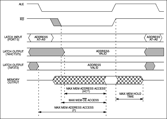
Figure 3. Data memory read.
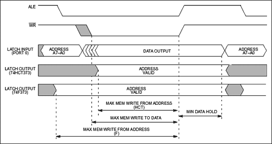
Figure 4. Data memory write.
Note that the term tMCS is used in the data sheet and in the equations that follow. It is a term that represents the time interval added for each stretch cycle. For example, if stretch is 0, then tMCS is zero and the equation remains the same. If stretch is one then tMCS equals 2tCLCL, and the equation is increased by this amount. The value of tMCS is increased by 4tCLCL for every additional stretch cycle.
Through analysis, it can be determined that there are four SRAM timing parameters that are necessary and sufficient to meet the timing requirements of the DS80C320 in most situations. For the following discussion of these requirements, the worst case timing conditions, i.e., a 33 MHz clock and zero stretch cycles, have been used. For a data read operation, the DS80C320 expects the time from an address change until valid data is available to be 64 ns (tAVDV1=3tCLCL-27) or less. If the propagation delay from D to Q of a 74F373 latch (8 ns) is subtracted from this parameter, you obtain a memory address access (tAA) requirement of 56 ns. Also for a read, the DS80C320 expects the time from the active-low RD signal going low until valid data is received from the memory to be 35 ns (tRLDV=2tCLCL-25) or less. Since the processor's active-low RD signal is tied to the memory's active-low OE pin, the memory must have an output enable access time (tOE) of less than 40 ns. After the DS80C320 has read the data, the SRAM must relinquish the bus within 25 ns (tRHDZ=tCLCL-5). This dictates that the SRAM parameter tOHZ be less than 25 ns. For a write, the processor will provide a minimum write pulse of 49 ns (tWLWH=2tCLCL-11), which is equal to the required minimum write pulse width (tWP) of the SRAM. On the basis of these four calculated parameters and assumed SRAM speeds shown in Table 2, the appropriate speed device may be determined for a number of different clock frequencies. A summary of the recommended RAM speeds is given in Table 3.
Table 2. Available RAM parameters
Table 3 illustrates the point that even with a 33 MHz clock, relatively slow SRAM devices may be selected if a single stretch cycle (default condition) is used. If performance is not the primary system consideration, or if it is but data memory accesses are an insignificant part of the overall processing requirements, the use of a stretch cycle may allow a more cost effective solution.
Table 3. Recommended RAM configuration

Figure 5. Fast EPROM turnoff.
All of the timing calculations used in this application note are based on the equations in the DS80C320 data sheet. The timing specifications given in the data sheet assume an approximately equal capacitive load on the signals specified. If the configuration of Figure 1 is used, this is achieved. If, however, any signal is connected to additional loads, then the capacitive loading including the additional devices should be evaluated. If there is a significant difference, additional margins should be used in the critical path analysis, and appropriate memory speeds selected.
For older or otherwise unconventional SRAM devices, it may be wise to confirm other important timing parameters such as data setup before write active. With the devices surveyed, meeting the four parameters discussed above will qualify the device for use.

1. For details on the equations presented in this document, refer to the DS80C320 data sheet.
2. tCLCL is the period of the crystal frequency, and is equal to 30.3 ns for a 33 MHz crystal.
Introduction
Dallas Semiconductor's DS80C320 processor provides extensive new application opportunities due to its increased throughput. The increased speed, however, also requires attention to the timing requirements of the memory that interfaces with the processor. This application note identifies the critical timing paths associated with the memory interface and identifies memory speeds required for various CPU crystal frequencies.A typical configuration for a DS80C320 processor system is shown in Figure 1. A 32K x 8 EPROM is used to hold program information, and a 8K x 8 Static RAM is used for data storage. The Least Significant Byte (LSB) of the memories' address is time multiplexed with data on processor pins AD7 through AD0. The signal ALE from the processor goes high before a new address is placed on the bus and goes low before it is removed. In Figure 1, the action of ALE going low is used to latch the address into a 74HCT373 8-bit transparent latch. The 74HCT373 then provides its latched address output to the memories while the AD7 through AD0 CPU bus carries data. The MSB of the address is not multiplexed, and is available on port pins P2.7 through P2.0 (A15-A9).

Figure 1. A typical DS80C320 system confirguration.
Program Memory
Some of the signals used in interfacing the DS80C320 with EPROM Program memory are shown in Figure 2. As can be seen, timing relationships for two latch technologies (HCT and F) are shown. The technology selected for this latch is critical to the memory selection. The 74HCT373 has a worst case propagation delay from input to output (D to Q) of 44 ns while the 74F373's is 8 ns. This results in significantly different memory address access timing requirements depending on the family used. Examining timing parameters from the DS80C320 data sheet reveals that an instruction must be ready to read into the processor within 60 ns (parameter itAVIV1=3tCLCL-27)1, assuming a 33 MHz clock2. If the 44 ns propagation delay through the HCT latch is subtracted from this, you arrive at a required address access time of 26 ns.
Figure 2. Program memory interface timing.
While EPROM devices with access times of 26 ns or less may be available, they are likely to be expensive. A simple and more cost effective approach to solving this timing constraint is to use a faster latch technology; an 74F373 for instance. Using the same analysis as above, if the propagation delay of the F373 latch, 8 ns, is subtracted from the tAVIV1 parameter (64 ns) you arrive at an address access requirement of 56 ns. This is much easier to realize than 26 ns.
There is another timing constraint that suggests the use of an "F" type part in faster applications. On a 74HCT373 latch, the minimum required hold time of the input after the latch enable (ALE) goes low may be as much as 13 ns. The latch's input, the address out of the processor, is held until it is driven by the memory's output. This output is enabled by active-low PSEN. Again referring to the data sheet, it can be seen that active-low PSEN may occur as quickly as 0.5 ns after ALE falls (parameter tLLPL). If the memory's output begins to drive the bus immediately after active-low PSEN enables it, then there may only be 0.5 ns hold time. That obviously violates the latch's requirement. While it is reasonable to assume that there will be some delay before the memory's output will drive the bus, this is not a specified (or tested) parameter. Therefore a conservative estimate of 5 ns will be assumed. From above numbers and the equation for the tLLPL parameter (0.25tCLCL-7), it can be calculated that clock frequencies of 19.23 MHz and below will allow sufficient hold time to satisfy the 74HCT373 latch's requirement. Note that the hold time for a 74F373 latch is 3 ns which is met under all conditions.
From the above analysis, you could choose 19.32 MHz as the latch technology switchover point, however, there is a reason why this was not done. Referring back to the address access equation (3tCLCL-24), it can be calculated that if a 74HCT373 latch is used for frequencies higher than 16.31 MHz, then a 90 ns or faster memory device is required. Therefore as a trade-off between latch speed and EPROM speed, the 74F373 latch (less expensive than a fast EPROM) is recommended for crystal frequencies greater than or equal to 16.31 MHz, and the 74HCT373 for lower frequencies.
As shown in Figure 1, active-low PSEN enables the EPROM's output, so the timing for this signal must also be considered when choosing a device. The DS80C320 data sheet specifies the time from active-low PSEN low to a valid instruction in must be no more than 70 ns (parameter tPLIV). This is therefore the maximum allowed access time from the memory's active-low OE pin. In summary, the two timing requirements for the selected EPROM are that the address access time must be less than 92 ns and the active-low OE access time must be less than 70 ns. When looking at EPROM data sheets, it can be seen that common access time combinations (address access, active-low OE access) are 55,35; 70,40; 90,40; 120,50; 150,65; 200,75; and 250,100 ns. The 55, 35 device meets both timing requirements for a 33 MHz clock on the DS80C320 and is the recommended selection.
Table 1 shows the slowest EPROM memory speeds recommended for various processor clock frequencies. If for some reason it is desirable to use devices faster than those recommended, this is possible. For this document, the memory speeds available (maximum access times from address and active-low OE respectively) are assumed to be those indicated above, however, any combination that meets the two requirements may be used. In Table 1, the memory speeds shown in bold are the recommended configurations.
Table 1. Recommended EPROM speeds
| CLOCK (MHZ) | MEMORY SPEED 74F373 | MEMORY SPEED 74HCT373 |
| 33.0 | 55 ns | — |
| 25.0 | 90 ns | — |
| 20.0 | 120 ns | 70 ns |
| 18.432 | 120 ns | 90 ns |
| 16.0 | 150 ns | 120 ns |
| 14.746 | 150 ns. | 120 ns |
| 14.318 | 150 ns | 120 ns |
| 12.0 | 200 ns | 150 ns |
| 11.059 | 200 ns | 200 ns |
| 7.37 | 250 ns | 250 ns |
| 1.8432 and below | 250 ns | 250 ns |
It should be noted that it is often possible to reduce the power consumption of EPROMs by keeping the active-low OE pin held active and controlling the device with the active-low CS pin. When doing this, however, the access time from active-low CS must be more closely considered. The active-low CS access time is often nearly the same value as the address access time (i.e., much slower than active-low OE access). If power consumption is the prime system consideration, a faster device may be selected, and the active-low CS used to select the chip.
Data Memory
Choosing a data memory (RAM) device to interface to the DS80C320 is much easier than choosing an EPROM device because of the flexibility designed into the processor. The DS80C320 provides a unique feature that allows the application software to adjust the speed at which data memory is accessed. The processor is capable of performing a MOVX instruction in as little as two instruction cycles (eight oscillator clocks). However, this value can be "stretched" as needed so that both fast memory and slow memory or peripherals can be accessed with no glue logic. On power up, the DS80C320 defaults to a stretch value of one resulting in a three cycle MOVX instruction. This default condition is a convenience to existing designs that may not have fast RAM in place. For the user who needs maximum performance, a stretch value of zero may be selected by software, resulting in a two machine cycle MOVX instruction. Even in high speed systems, it may not be necessary or desirable to perform data memory accesses at full speed. Additionally, there are a variety of memory mapped peripherals such as LCD displays or UARTs that are not fast enough to keep up with the full speed DS80C320. This flexibility allows the user to trade some performance for slower data RAMs if so desired.For maximum performance, i.e., with a two machine cycle data memory access programmed into the processor, the fetch of a MOVX instruction takes one machine cycle leaving one machine cycle for the memory read or write. For the analysis of the data memory's timing requirements that follows, it will be assumed that the recommendations of Table 1 have been followed. This implies that a 74F373 latch is used for clock frequencies above 16.31 MHz. A diagram of a single cycle data memory read is shown in Figure 3 and a single cycle data memory write is shown in Figure 4.

Figure 3. Data memory read.

Figure 4. Data memory write.
Note that the term tMCS is used in the data sheet and in the equations that follow. It is a term that represents the time interval added for each stretch cycle. For example, if stretch is 0, then tMCS is zero and the equation remains the same. If stretch is one then tMCS equals 2tCLCL, and the equation is increased by this amount. The value of tMCS is increased by 4tCLCL for every additional stretch cycle.
Through analysis, it can be determined that there are four SRAM timing parameters that are necessary and sufficient to meet the timing requirements of the DS80C320 in most situations. For the following discussion of these requirements, the worst case timing conditions, i.e., a 33 MHz clock and zero stretch cycles, have been used. For a data read operation, the DS80C320 expects the time from an address change until valid data is available to be 64 ns (tAVDV1=3tCLCL-27) or less. If the propagation delay from D to Q of a 74F373 latch (8 ns) is subtracted from this parameter, you obtain a memory address access (tAA) requirement of 56 ns. Also for a read, the DS80C320 expects the time from the active-low RD signal going low until valid data is received from the memory to be 35 ns (tRLDV=2tCLCL-25) or less. Since the processor's active-low RD signal is tied to the memory's active-low OE pin, the memory must have an output enable access time (tOE) of less than 40 ns. After the DS80C320 has read the data, the SRAM must relinquish the bus within 25 ns (tRHDZ=tCLCL-5). This dictates that the SRAM parameter tOHZ be less than 25 ns. For a write, the processor will provide a minimum write pulse of 49 ns (tWLWH=2tCLCL-11), which is equal to the required minimum write pulse width (tWP) of the SRAM. On the basis of these four calculated parameters and assumed SRAM speeds shown in Table 2, the appropriate speed device may be determined for a number of different clock frequencies. A summary of the recommended RAM speeds is given in Table 3.
Table 2. Available RAM parameters
| tAA (ns) | tOE (ns) | tOHZ (ns) | tWP (ns) |
| 60 | 35 | 25 | 45 |
| 70 | 35 | 30 | 45 |
| 80 | 35 | 30 | 60 |
| 100 | 50 | 35 | 60 |
| 120 | 60 | 45 | 70 |
| 150 | 55 | 40 | 90 |
| 170 | 80 | 35 | 120 |
| 200 | 100 | 35 | 150 |
Table 3 illustrates the point that even with a 33 MHz clock, relatively slow SRAM devices may be selected if a single stretch cycle (default condition) is used. If performance is not the primary system consideration, or if it is but data memory accesses are an insignificant part of the overall processing requirements, the use of a stretch cycle may allow a more cost effective solution.
Table 3. Recommended RAM configuration
| CLOCK (MHz) | LATCH | MEMORY SPEED (zero stretch) |
MEMORY SPEED (one stretch) |
| 33.0 | F373 | 55 ns | 120 ns |
| 25.0 | F373 | 80 ns | 200 ns |
| 20.0 | F373 | 120 ns | 200 ns |
| 18.432 | F373 | 120 ns | 200 ns |
| 16.0 | HCT373 | 170 ns | 200 ns |
| 14.746 | HCT373 | 170 ns | 200 ns |
| 14.318 | HCT373 | 200 ns | 200 ns |
| 12.0 | HCT373 | 200 ns | 200 ns |
| 11.059 | HCT373 | 200 ns | 200 ns |
| 7.37 | HCT373 | 200 ns | 200 ns |
| 1.8432 and below | HCT373 | 200 ns | 200 ns |
Additional Considerations
In developing this application note, it was noted that some EPROM devices have extremely long "turn off" times. If the EPROM selected for 33 MHz systems has an "output disable to float" time greater than 25 ns (parameter tPXIZ=tCLCL-5), bus contention will occur on the processor's AD7-AD0 bus. In most situations, this simply results in higher power consumption. However, in some situations the address setup time to the memory can be affected necessitating a faster memory. The simplest solution to this problem is to use a device with the required turn-off time, but another possible solution exists. A 74F244 driver can be placed between the EPROM's output and the processor's data bus as shown in Figure 5. The 74F244's outputs turn off within a maximum of 8 ns, thereby releasing the processor's bus almost immediately and eliminating the contention.
Figure 5. Fast EPROM turnoff.
All of the timing calculations used in this application note are based on the equations in the DS80C320 data sheet. The timing specifications given in the data sheet assume an approximately equal capacitive load on the signals specified. If the configuration of Figure 1 is used, this is achieved. If, however, any signal is connected to additional loads, then the capacitive loading including the additional devices should be evaluated. If there is a significant difference, additional margins should be used in the critical path analysis, and appropriate memory speeds selected.
For older or otherwise unconventional SRAM devices, it may be wise to confirm other important timing parameters such as data setup before write active. With the devices surveyed, meeting the four parameters discussed above will qualify the device for use.
Equation Summary
For the user who wishes to calculate the memory speed requirements using a crystal frequency not shown in the preceding tables, the following equations provide a concise summary of the information needed. These times are for zero stretch cycles. The memory devices selected must have an address access time (based on the use of an F373 or an HCT373), an active-low OE access time, a active-low WE time, and a bus release time less than or equal to the calculated values. Note again that tCLCL is the period of the clock.
1. For details on the equations presented in this document, refer to the DS80C320 data sheet.
2. tCLCL is the period of the crystal frequency, and is equal to 30.3 ns for a 33 MHz crystal.
 電子發燒友App







評論