The MAX104 processes analog input bandwidths that exceed 2.2GHz with 8-bit resolution. It sets a new standard for performance in high-frequency, high-bandwidth digital communications receivers, digital oscilloscopes, and high-speed data-acquisition systems.
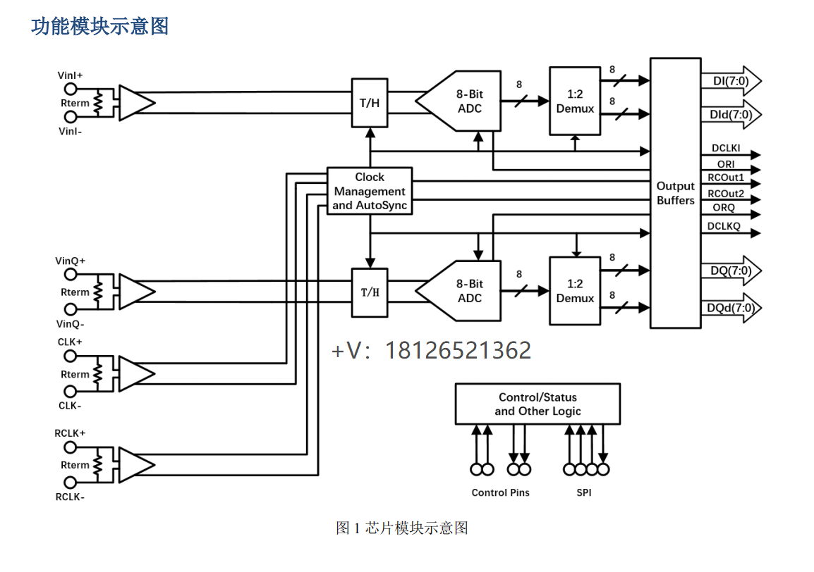
The MAX104 is a fast silicon monolithic analog-to-digital converter (ADC) that integrates a high-bandwidth track/hold (T/H) amplifier (Figure 1) with a high-speed quantizer that supports accurate digitizing of wideband analog input signals from DC to 2.2GHz. It is based on Maxim's GST-2 Giga-Speed silicon-bipolar process technology. This high-speed, self-aligned double-polysilicon process has been developed for high-density, high-performance circuits. It employs many of the features, such as trench isolation, that are incorporated in Maxim's lower performance GST-1 process.
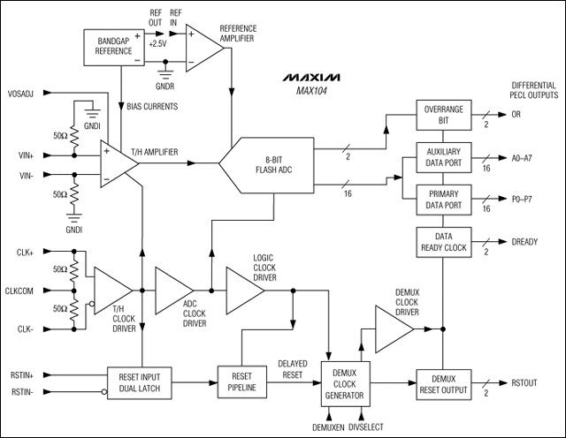
Figure 1. This simplified block diagram shows how the MAX104 integrates a high-bandwidth T/H amplifier with a high-speed quantizer.
Although many of the outstanding performance parameters of the MAX104 are possible with the integrated-circuit process (such as a transition frequency of 27GHz for NPN transistors, a three-metal interconnect system, small geometry, and precision laser-trimmed nickel-chrome (NiCr) thin-film resistors), additional credit goes to the MAX104's design team for creating an efficient and effective ADC architecture.
Most high-speed ADCs that sample more than several hundred megahertz have input bandwidths that are limited to no more than their maximum sampling frequency to improve noise performance. One example is the signal-to-noise ratio (SNR). This limited input bandwidth may rule out use in applications where bandwidths of interest in the input spectrum are higher, and an undersampling approach is needed. Also, if the input signal is changing rapidly during conversion, the effective number of bits (ENOB) and SNR will be reduced. The MAX104's on-chip 2.2GHz full-power-bandwidth T/H amplifier (Figure 2) increases dynamic performance significantly and supports more precise capture of fast analog data at extremely high conversion rates.
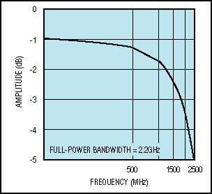
Figure 2. The MAX104's full-power bandwidth is shown as a function of input amplitude.
Bandgap Reference
The MAX104 features an on-board +2.5V precision bandgap reference, which can be activated by connecting the bandgap reference's output contact (REFOUT) to the in-phase input (REFIN) of the internal reference amplifier. The negative input of this amplifier is internally tied to the reference ground (GNDR).The REFOUT port can provide a current of up to 2.5mA for external devices. This is enough drive for two MAX104s configured for interleaved operation (to achieve a sampling rate of 2 gigasamples per second, or 2Gsps). Since the bandgap reference source is internally compensated, external bypass components are not needed with REFOUT connections.
To overdrive the internal reference, an external precision reference can be connected to the REFIN pin with REFOUT left floating. The external reference may then be used to adjust the full-scale range of the MAX104.
The MAX104's T/H amplifier input circuit design reduces the input signal requirement and supports a full-scale signal input range of 500mV peak-to-peak. Obtaining a full-scale digital output with a differential input requires 250mV applied between the positive (VIN+) and the negative input (VIN-) pins. Midscale digital output codes occur at an input of 0V.
For a zero-scale digital output code, the negative input (VIN-) must be 250mV above the positive input (VIN+). The high-performance differential T/H amplifier enables the MAX104 to be used in single-ended input configurations without any degradation in dynamic performance. For a typical single-ended configuration, the analog input signal is coupled to the T/H amplifier stage at the in-phase input pad (VIN+), while the inverted phase input (VIN-) pad is referenced to ground. Single-ended operation supports an input amplitude of 500mV peak-to-peak, centered at approximately 0V. For minimizing reflections and improving performance, the MAX104 inputs feature impedance-matched, on-chip, laser-trimmed 50Ω NiCr termination resistors.
Demonstrating almost identical dynamic performance at analog input frequencies of 125MHz (Figure 3), 250MHz, 500MHz (Figure 4), and 1GHz (Figure 5) with a sampling rate of 1Gsps for differential and single-ended analog input operation, the MAX104 solves one of the most perplexing problems in high-speed ADC applications—the need for costly, space-consuming, single-ended-to-differential signal-conversion circuitry. Now, applications requiring single-ended signal sources can just feed this signal into the VIN+ pin and terminate the VIN- pin through a 50Ω resistor connected to ground.
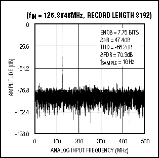
Figure 3. This fast Fourier transform (FFT) demonstrates the over-sampled performance of the MAX104 at a sampling rate of 1Gsps and an analog input frequency of 125MHz.
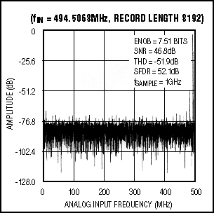
Figure 4. This FFT was taken at a Nyquist frequency of 500MHz and a sampling rate of 1Gsps.
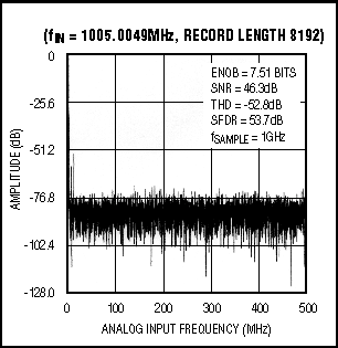
Figure 5. This FFT was measured with the MAX104 undersampling an analog input frequency of 1GHz at a sampling rate of 1Gsps.
Similar to its analog input structure, the MAX104 features clock inputs designed for either single-ended or differential operation with very flexible input-drive requirements. Each clock input is terminated with an on-chip, laser-trimmed, 50Ω precision NiCr resistor to the clock-termination return. This termination may be connected anywhere between ground and -2V for compatibility with standard emitter-coupled-logic (ECL) drive levels.
The clock inputs are internally buffered with an amplifier to ensure proper operation of the ADC even with small-amplitude sine-wave sources. The MAX104 was designed for single-ended operation, maintaining superior dynamic performance when using low-phase-noise sine-wave clock input signals with as little as 100mV amplitude.
To obtain the lowest jitter clock drive, a low-phase-noise sine-wave source can be AC- or DC-coupled into a single clock input. The MAX104 can accommodate clock amplitudes up to 1V (2V peak-to-peak) with the clock-termination return connected to ground. The dynamic performance of the ADC is essentially unaffected by clock signal amplitudes from 100mV to 1V.
The ADC can be driven from a standard differential ECL clock source by simply setting the clock-termination voltage to -2V. To maintain the best performance, a very- high-speed differential ECL driver should be used.
Clock inputs CLK+ and CLK- may also be driven with positive referenced ECL (PECL) logic levels if the clock inputs are AC coupled. A single-ended ECL drive can also be used if the undriven clock input is connected to the ECL VTT voltage (nominally -1.3V).
Another useful feature of the MAX104 may be its internal output demultiplexer (demux) circuitry. This circuitry provides three different modes of operation. The demux operation is controlled by two transistor-transistor-logic (TTL)/complementary-metal-oxide-semiconductor (CMOS)-compatible digital inputs: DEMUXEN, which activates or deactivates the internal demux, and DIVSELECT, which selects one of three demux modes (DIV1, DIV2, or DIV4).
The DIV2 (demux) mode reduces the output data rate to one-half the sample clock rate. The demuxed outputs are presented in dual 8-bit format with two consecutive samples in the primary and auxiliary output ports on the rising edge of the data-ready clock. The DIV1 nondemultiplexed (nondemux) mode supports operation of the MAX104 at sampling speeds up to 500 megasamples per second (Msps). In this mode, the internal demux is disabled and the sampled data are presented to the primary output port only. To consume less power, the auxiliary port can be shut down by two separate inputs (AUXEN1 and AUXEN2). To save additional power, the external 50Ω termination resistors connected to the logic PECL power supply (VCCO at -2V) can be removed from all auxiliary output ports.
In a special decimated, demuxed output mode (DIV4), the MAX104 discards every other input sample and outputs data at one quarter of the input sampling rate. This mode is particularly useful for system debugging using the resulting slower output data rates. With an input clock of 1GHz, the effective output data rate will be reduced to 250MHz in this mode.
Along with the on-chip demux, the MAX104 provides internal demux reset circuitry that enables multiple ADCs to be synchronized for proper interleaving operation. In addition, the reset signal appears as an external demux reset output for synchronizing external demuxes.
Furthermore, the MAX104 provides latched, differential PECL outputs, which make the ADC ideal for driving controlled low-impedance lines. The PECL outputs can be powered from +3V to +5.25V DC supply voltages. PECL outputs on the MAX104 are typically terminated with a parallel 50Ω termination resistor into VTT = VCCO - 2V (the PECL termination voltage).
Primary port outputs are labeled P0–P7 (LSB to MSB), while the auxiliary ports are labeled A0–A7. Outputs DREADY+ and DREADY- are data-ready true and complementary outputs, supplying the data clock.
These signal lines are used to latch the output data from the primary to the auxiliary output ports, as well as supplying a synchronous clock for downstream digital circuitry, such as demuxes or high-speed memory devices. Data changes are triggered on the rising edge of the DREADY clock.
Outputs OR+ and OR- are overrange true and complementary outputs. Outputs RSTOUT+ and RSTOUT- are the reset-out true and complementary outputs provided to reset downstream circuitry.
The MAX104 is supplied in a 192-contact enhanced-super-ball-grid-array (ESBGA) package from Amkor/Anam (Chandler, AZ) that measures 25mm x 25mm. The MAX104 provides an on-board 1:2 demux function, slowing data rates to 500Mbps supplied on two ports. The package features 50Ω microstrip interconnects from the solder balls to the bond wires, which support high input/output (I/O) operating frequencies. In addition, the package enables a large number of solder balls to be dedicated to power supplies and ground. With a thickness of only 1.4mm, this 1.27mm pitch ESBGA package saves circuit-board space while providing excellent thermal performance. In many applications, the MAX104 can be used without a heat sink.
The MAX104 is ideal for many applications where high sampling rates are required to either capture an instantaneous value from a fast-moving signal, such as in a high-speed data acquisition (DAQ) application, or to digitize a complex high-frequency, high-bandwidth signal. One example of this is in wideband digital receivers for digital base stations. In this case, signal bandwidths that exceed 300MHz are allowed to pass through the receiver intermediate-frequency (IF) stages to the demodulator. At this point, the information bandwidth may be filtered and amplified before being presented to the ADC front end. This approach, known as block or direct downconversion, requires that the input bandwidth of the ADC be sufficiently flat to prevent distortions and nonlinearities in the resulting digital representation. The high-speed data stream thus created is then presented to a digital demodulator which separates the individual channels and extracts the modulated information.
Applying the ADC
The exceptional SNR and spurious-free dynamic-range (SFDR) performance of the MAX104 at input frequencies below (e.g., at 125MHz and 250MHz) and well above the Nyquist frequency (e.g., operating at 1GHz) make the MAX104 the converter of choice for oversampled as well as undersampled 8-bit digital communications applications. For instance, the MAX104 delivers a 47.4dB SNR and 68.9dB SFDR at an analog input frequency of 125MHz. The two-tone performance is an impressive -57.7dB at the same test frequency.Another ideal application is in DAQ instruments and systems. These are systems that are designed to sample, analyze, and display signal waveforms detected at various nodes within a circuit under analysis (e.g., high-speed, multichannel digital oscilloscopes). ADCs are used in the front-end circuitry of digital sampling oscilloscopes (DSOs). Often, multiple converters are time interleaved to increase an effective sampling frequency. Maxim's new 600Msps/1.5Gsps converter, the MAX106, provides designers with the options of lower and even higher sampling speeds.
Important data-converter specifications in DAQ applications include an analog signal input bandwidth, gain flatness, ENOB performance, and low occurrence of metastable states. A differential comparator design and its decoding circuitry reduce out-of-sequence code errors, such as thermometer bubbles or sparkle codes, and provide excellent metastable performance of less than one error per 1016clock cycles. Unlike other ADCs, which may have errors that result in false full-scale or zero-scale outputs, the MAX104 keeps its error magnitude to no more than 1LSB.
Furthermore, this fast ADC accomplishes outstanding numbers for integral-nonlinearity (INL) and differential-nonlinearity (DNL) parameters, ensuring monotonic operation. After trimming, the MAX104 displays parameters as low as ±0.25LSB (Figures 6, 7).
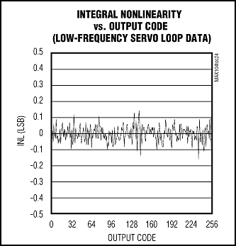
Figure 6. The MAX104's typical integral nonlinearity.
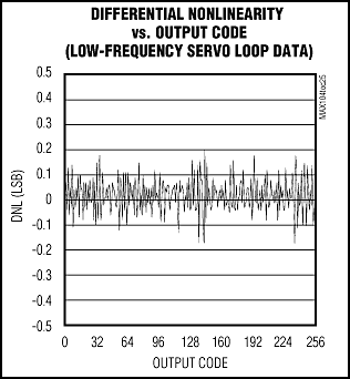
Figure 7. The MAX104's typical differential nonlinearity.
A similar version of this article appeared in the March 1999 issue of Microwaves and RF.
 電子發(fā)燒友App




評(píng)論