Abstract: This application note describes the basic information needed for a Software Engineer to convert an application from a sector-erasable (SE) to a page-erasable (PE) MAXQ microcontroller. This information applies to the MAXQ flash-based microcontrollers that are available in both SE and PE versions.
There are several reasons for transitioning from SE to PE flash devices, but most commonly it is the need to reduce costs or start development work using currently available devices. This application note provides the information to make the transition as quick and smooth as possible.
To determine the flash types available on your MAXQ7665, please refer to the data sheet. For more detailed information using the SE and PE data and program flash, refer to the application notes in the Table 1.
Table 1. SE and PE Flash Application Note Reference Table
Table 2. Flash Structure and Performance Overview
Table 3. SE and PE Routine Mapping
Notes
1 The one-word-erase feature is available for the MAXQ7665C device only. For more information, see application note 3579, noted in Table 1.
Table 4. SE Flash Memory Maps for MAXQ7665

Table 5. PE Flash Memory Maps for MAXQ7665
The PE flash has a separate set of routines that manage the data and program flash memory. These separate routines are necessary because the page structures differ between data and program flash memories. Only the flashEraseAll() routine operates on both data and program flash pages. There are also additional page-erase routines that allow smaller blocks of flash to be erased at a time. PE flash is different than SE flash when writing to program flash as you must write an entire page at once. Please refer to the application notes listed in Table 1 for detailed descriptions of the Utility ROM flash routines.
Unlike the SE flash flashWrite() routine that writes one word at a time, the flashWrite()routine used for writing to PE program flash memory writes 1 page (32 words) at a time. This larger code size should not pose a problem for converting the software originally written for SE program flash over to support PE flash—program code is normally written in large blocks anyway.
Table 6. SE Flash Utility ROM Routines
Table 7. PE Flash Utility ROM Routines
Table 8. Map of PE and SE Flash Utility ROM Functions
Figure 2 shows the structure of the 1kB PE data flash which consists of eight sectors, each sector containing 64 pages, each page containing one word. A PE operation will erase two consecutive pages (two words). The two-word page-erase of the PE data flash provides greater flexibility in architecting a fault-tolerant data-storage mechanism.
The Utility ROM also contains routines for the MAXQ7665C, which supports one-word-erase/write operation. The flashWriteE() and flashReadE() routines enable EEPROM-like one-word-erase/write functionality in this device. See the MAXQ7665 User's Guide and Application Note 3579 (in Table 1) for more details.
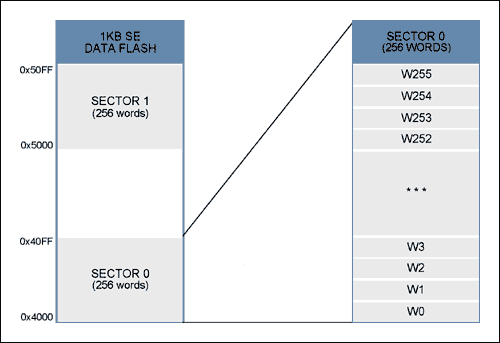
Figure 1. 1kB SE Data Flash—Sector Structure.

Figure 2. 1kB PE Data Flash—Sector/Page Structure.
Table 9. Example of a Bounded-Queue Memory Map

Figure 3. Bounded Queue with Bank Switch Flow for SE Flash.
The constants and data structures for the example in Figure 3 are defined below:
Table 10. Example of a PE Flash Bounded-Queue Memory Map
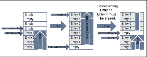
Figure 4. Bounded-Queue Flow for PE Flash.
The updated constants and data structures are defined below. The entry data structure stays the same, but anything used for bank switching has been removed:
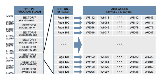
Figure 5. 32kB PE Program Flash—Sector/Page Structure.
The Figure 6 flowcharts show both SE and PE reflash routines. Typically when reflashing the main application, the first step is to erase the entire main application code area with a call to a user-written function like flashEraseApplication(), which calls flashEraseSector() for each sector used to store the main application code. The method for erasing PE flash is essentially the same, except that smaller amounts flash are erased with a single call. As a result, more calls to flashEraseSector() and/or flashErasePage() will occur.
Problems can occur when porting the flash write loop. The PE flash write function, flashWrite(), writes a full page (32 words) at a time. Depending on how the data is to be written, this section of the code may need to be rewritten to accommodate the collection of one page of program data for each call to flashWrite(). If the application requires the least impact on higher level communications protocols, then writing a routine to emulate the single-word write of the SE flashWrite() function is the best approach. See Figure 7 for the updated PE reflash flowchart that emulates the SE reflash flow. When using this approach, write requests must come in groups of 32 words so the application space should always be a multiple of 32 words.

Figure 6. Flowcharts of Very Simple Reflash Routines.
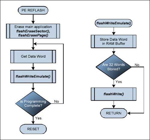
Figure 7. Emulating SE Flash Flow.
The following code is a simple reflash routine for a device with SE flash that receives commands and data through an unspecified serial link. Remember that this routine can not be located in the same sector of flash that is being reprogrammed.
Introduction
This application note outlines the differences between the sector-erasable (SE) and page-erasable (PE) flash memories used in some MAXQ7665 microcontrollers The article also explains the basic steps to convert an application from SE to PE flash versions. The SE flash is available on microcontrollers with greater than 32kB program flash as a more cost-effective solution over PE flash.There are several reasons for transitioning from SE to PE flash devices, but most commonly it is the need to reduce costs or start development work using currently available devices. This application note provides the information to make the transition as quick and smooth as possible.
To determine the flash types available on your MAXQ7665, please refer to the data sheet. For more detailed information using the SE and PE data and program flash, refer to the application notes in the Table 1.
Table 1. SE and PE Flash Application Note Reference Table
| AN # | Application Note Title |
| 3575 | In-Application Programming (IAP) of the MAXQ7665 Sector-Erasable Program and Data Flash |
| 3576 | In-Application Programming (IAP) of the MAXQ7665 Page-Erasable (PE) Program and Data Flash |
| 3579 | In-Application Programming (IAP) of the MAXQ7665C Page-Erasable (PE) Flash with One Word Erase Data Flash |
SE and PE Flash Compared
This section summarizes the differences between SE and PE flash.Table 2. Flash Structure and Performance Overview
| Data Flash | SE | PE |
| Structure: | 2 sectors: 256W or 512W | 4 or 8 sectors: 64 pages/sector containing 1W |
| Erase: | 1 Sector | 2 Pages—2 Words or 1 Page—1 Word1 |
| Write: | 1 Word | 1 Word |
| Program Flash | SE | PE |
| Structure: | 1 or 2 sectors: 16kW or 32kW | 4 or 8 sectors: 64 pages/sector containing 32W |
| Erase: | 1 Sector | 2 Pages—64 Words |
| Write: | 1 Word | 32 Words |
Table 3. SE and PE Routine Mapping
| PE Flash | SE Flash | ||
| Routine # | Function Name | Routine # | Function Name |
| 1 | flashWrite() | 15 | flashWrite() |
| 2 | flashErasePage() | ||
| 3 | flashEraseAll() | 3 | flashEraseAll() |
| 4 | moveDP0() | 4 | moveDP0() |
| 16 | flashEraseSector() | 2 | flashEraseSector() |
| 17 | dataFlashWrite() | 15 | flashWrite() |
| 18 | dataFlashWriteE()1 | ||
| 15 | flashWrite() | ||
| 19 | dataFlashErasePage() | ||
| 20 | dataFlashEraseSector() | 2 | flashEraseSector() |
| 21 | dataFlashEraseAll() | ||
| 22 | dataFlashReadE()1 | 4 | moveDP0() |
Notes
1 The one-word-erase feature is available for the MAXQ7665C device only. For more information, see application note 3579, noted in Table 1.
Memory Map Comparison
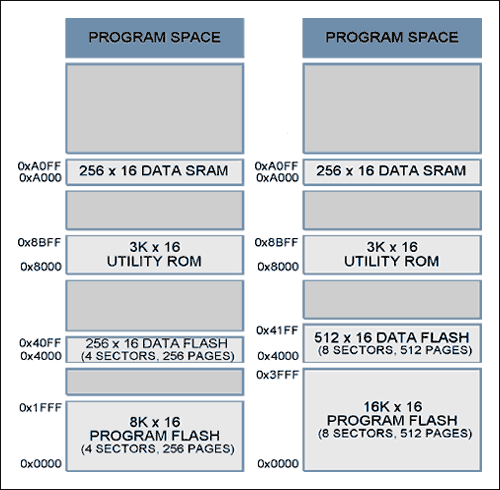
Tables 4 and 5 show the flash memory maps for the 16kB and 32kB versions of the MAXQ7665. Refer to the data sheet for a complete list of memory options. The SE flash contains a second data flash sector located at 0x5000. This data sector is normally used for implementing bank-switching methods to support fault-tolerant in-system data storage. The PE flash version does not need the second data sector to implement fault-tolerant in-system data storage.Table 4. SE Flash Memory Maps for MAXQ7665

Table 5. PE Flash Memory Maps for MAXQ7665

Utility ROM Flash Routine Differences
It is important to understand how the low-level flash routines differ between the SE and PE flash types. Tables 6 and 7 show the flash routines supplied by the Utility ROM for both flash types. Table 8 shows how each PE flash function maps to its SE flash counterpart. For a complete listing of Utility ROM routines, refer to the User's Guide for the specific MAXQ part used.The PE flash has a separate set of routines that manage the data and program flash memory. These separate routines are necessary because the page structures differ between data and program flash memories. Only the flashEraseAll() routine operates on both data and program flash pages. There are also additional page-erase routines that allow smaller blocks of flash to be erased at a time. PE flash is different than SE flash when writing to program flash as you must write an entire page at once. Please refer to the application notes listed in Table 1 for detailed descriptions of the Utility ROM flash routines.
Unlike the SE flash flashWrite() routine that writes one word at a time, the flashWrite()routine used for writing to PE program flash memory writes 1 page (32 words) at a time. This larger code size should not pose a problem for converting the software originally written for SE program flash over to support PE flash—program code is normally written in large blocks anyway.
Table 6. SE Flash Utility ROM Routines
| Routine Number | Routine Name | Entry Point ROMTable = ROM[800Dh] |
Entry Point Physical Address |
| 2 | flashEraseSector() | ROM[ROMTable + 1] | 0x8XXX |
| 3 | flashEraseAll() | ROM[ROMTable + 2] | 0x8XXX |
| 4 | moveDP0() | ROM[ROMTable + 3] | 0x8XXX |
| 15 | flashWrite() | ROM[ROMTable + 14] | 0x8XXX |
Table 7. PE Flash Utility ROM Routines
| Routine Number | Routine Name | Entry Point ROMTable = ROM[800Dh] |
Entry Point Physical Address |
| 1 | flashWrite() | ROM[ROMTable] | 0x8XXX |
| 2 | flashErasePage() | ROM[ROMTable + 1] | 0x8XXX |
| 3 | flashEraseAll() | ROM[ROMTable + 2] | 0x8XXX |
| 4 | moveDP0() | ROM[ROMTable + 3] | 0x8XXX |
| 16 | flashEraseSector() | ROM[ROMTable + 15] | 0x8XXX |
| 17 | dataFlashWrite() | ROM[ROMTable + 16] | 0x8XXX |
| 18 | dataFlashWriteE() | ROM[ROMTable + 16] | 0x8XXX |
| 19 | dataFlashErasePage() | ROM[ROMTable + 18] | 0x8XXX |
| 20 | dataFlashEraseSector() | ROM[ROMTable + 19] | 0x8XXX |
| 21 | dataFlashEraseAll() | ROM[ROMTable + 20] | 0x8XXX |
| 22 | dataFlashReadE() | ROM[ROMTable + 21] | 0x8XXX |
Table 8. Map of PE and SE Flash Utility ROM Functions
| PE Flash | SE Flash |
| u16 flashWrite(u16 *pDest, u16 *pSrc) | u16 flashWrite(void *pAddress, u16 iData) |
| u16 flashErasePage(void *) | |
| u16 flashEraseSector(void *) | u16 flashEraseSector(void *) |
| moveDP0 | moveDP0 |
| u16 flashEraseAll(void) | u16 flashEraseAll(void) |
| u16 dataFlashWrite(u16 *pAddress, u16 iData) | u16 flashWrite(void *pAddress, u16 iData) |
| u16 dataFlashWriteE(u16 *pAddress, u16 iData) | u16 flashWrite(void *pAddress, u16 iData) |
| u16 dataFlashErasePage(void *) | |
| u16 dataFlashEraseSector(void *) | u16 flashEraseSector(void *) |
| u16 dataFlashEraseAll(void) | |
| u16 dataFlashReadE(u16 *pAddress) | moveDP0 |
Data Flash
It should normally be a simple task to port software written for SE flash over to operate with PE flash. When the differences between the two data-flash structures are understood, the best approach for the porting task emerges. Figure 1 shows the structure of the SE data flash, which consists of two sectors each with 256 words. An erase operation erases the entire contents of one sector, while one word can be written at a time. There are two sectors available to implement bank switching for applications requiring a fault-tolerant data storage mechanism. When bank switching is needed, the effective flash data size is only one sector.Figure 2 shows the structure of the 1kB PE data flash which consists of eight sectors, each sector containing 64 pages, each page containing one word. A PE operation will erase two consecutive pages (two words). The two-word page-erase of the PE data flash provides greater flexibility in architecting a fault-tolerant data-storage mechanism.
The Utility ROM also contains routines for the MAXQ7665C, which supports one-word-erase/write operation. The flashWriteE() and flashReadE() routines enable EEPROM-like one-word-erase/write functionality in this device. See the MAXQ7665 User's Guide and Application Note 3579 (in Table 1) for more details.

Figure 1. 1kB SE Data Flash—Sector Structure.

Figure 2. 1kB PE Data Flash—Sector/Page Structure.
Porting Example: Bounded Queue with Bank Switching
The following example illustrates how a bounded-queue technique with bank-switching architecture designed for a SE data flash can be easily modified to work with a PE data flash. A SE data sector size of 256 x 16 is used for this example. Each sector will hold up to eight entries of 32 words. Table 9 shows the memory map for each sector. Figure 3 shows how the entries will be written into the SE data flash.Table 9. Example of a Bounded-Queue Memory Map
| FQueueBank0[ ] | |
| Queue Index | Data Flash |
| 7 | 0x40E0-0x40FF |
| 6 | 0x40C0-0x4FDF |
| 5 | 0x40A0-0x40BF |
| .... | .... |
| 2 | 0x4040-0x405F |
| 1 | 0x4020-0x403F |
| 0 | 0x4000-0x401F |
| FQueueBank1[ ] | |
| Queue Index | Data Flash |
| 15 | 0x50E0-0x50FF |
| 14 | 0x50C0-0x5FDF |
| 13 | 0x50A0-0x50BF |
| .... | .... |
| 10 | 0x5040-0x505F |
| 9 | 0x5020-0x503F |
| 8 | 0x5000-0x501F |

Figure 3. Bounded Queue with Bank Switch Flow for SE Flash.
The constants and data structures for the example in Figure 3 are defined below:
Variables and Constants
#define C_Q_BANKSIZE      (  8 )  // The number of entries in each bank
#define C_Q_BANKS         (  2 )     // The number of banks
#define C_Q_ERASE_THRESH  ( C_Q_BANKSIZE - 2 )
#define C_Q_MAX           ( C_Q_BANKSIZE * C_Q_BANKS )
#define C_Q_MAX_ID        ( C_Q_MAX * 2 )
#define C_Q_DATASIZE      ( 31 )     // Data size in words
#define C_Q_FULL          ( -1 )
#define C_Q_XSUM_ERROR    ( -2 )
#define C_FLASH_EMPTY     ( 0xFF )

// For this example each entry is 31 words of arbitrary data.
typedef struct {
    u16 iData[C_Q_DATASIZE];
    u8 iID;
    u8 iChecksum;
} QENTRY;

extern bool ChecksumValid(QENTRY *pEntry);
extern u16 flashEraseSector(void *pAddress);
extern u16 flashWrite(void *pAddress, u16 iData);

extern QENTRY FQueueBank0[C_Q_MAX]; // Mapped to SE data flash sector 0
extern QENTRY FQueueBank1[C_Q_MAX]; // Mapped to SE data flash sector 1
extern u8 iQID;                     // ID number of the last entry
extern u8 iQIndex;                  // Index of current entry
extern u8 iBank;                    // Index of current flash bank

QENTRY *FQueue[C_Q_BANKS] = {FQueueBank0, FQueueBank1};
The initialization routine follows below.Initialization Code
/*
// queueInitialize()
//    This routine returns the current valid entry in the queue and
//    sets the global variable iQID to the ID of the current valid entry.
*/
short queueInitialize(void)
{
s16 iIndex;
    iQID = 0;
    // Find the active sector
    for (iBank=0;iBank < C_Q_BANKS; ++iBank)
    {
        // Only the current sector will have the first entry used
        // and the last entry empty.
        if (FQueue[iBank][0].iID != C_FLASH_EMPTY &&
            FQueue[iBank][C_Q_BANKSIZE-1].iID == C_FLASH_EMPTY) {

            // Find the last valid entry.
            for (iIndex=1;iIndex < C_Q_BANKSIZE-1; ++iIndex)
            {
                if (FQueue[iBank][iIndex].iID == C_FLASH_EMPTY)
                {
                    iQID = FQueue[iBank][iIndex-1].iID;
                    return iIndex - 1 + C_Q_BANKSIZE*iBank;
                }
            }
        }
    }

    // Should never get here. The queue is full, return error.
    return C_Q_FULL;
}
The write routine code is shown next.Write Data Code
/*
// queueWriteEntry()
//    Writes new entry into the flash queue.
*/
short queueWriteEntry(QENTRY *pEntry)
{
void *pDest;
u16 i;
    if (pEntry != NULL)
    {
        // Compute the new packet ID.
        iQID = (iQID + 1) % C_Q_MAX_ID;

        // Compute the new Index.
        iQIndex = (iQIndex + 1) % C_Q_MAX;

        // Set the packet ID.
        pEntry->iID = iQID;

        // Calculate the checksum.
        pEntry->iChecksum = iQID;
        for (i = 0; i < C_Q_DATASIZE; ++i)
            pEntry->iChecksum += pEntry->iData[i];

        // Write packet to flash.
        pDest = &FQueue[iQIndex / C_Q_BANKSIZE][iQIndex % C_Q_BANKSIZE];
        for (i = 0; i < sizeof(QENTRY)/2; ++i)
            flashWrite(pDest, ((u16 *)pEntry)[i]);
        return true;
    }
    return false;
}
Finally, the erase sector routine needs to be called at least once after every write to ensure that the next sector to be used will be erased.Erase Sector Maintenance Code
/*
// queueEraseSectorMaintenance()
//    This routine monitors the flash sectors and, when the current sector is
//    almost full, it erases the next sector to free up more room.
//    Returns true if a sector erase occurred during the call.
//
//    This routine must be called at least once per queueWriteEntry() call.
*/
bool queueEraseSectorMaintenance(void)
{
    // If the sector is almost full then we want to try and erase the next
    // sector.
    if ((iQIndex % C_Q_BANKSIZE) > C_Q_ERASE_THRESH)
    {
        short iBank = (iQIndex / C_Q_BANKSIZE + 1) % C_Q_BANKS;

        // If there are restrictions on when flash can be erased
        // then additional conditional can be added here.
        // Just make sure that the next sector is erased before the current
        // sector is full.
        if (FQueue[iBank][0].iID != C_FLASH_EMPTY)
        {
            flashEraseSector(FQueue[iBank]);
            return true;
        }
    }
    return false;
}
Now the task is to convert this very simple example for use on a 256 x 16 PE data flash. Bank switching is not needed for the PE data flash since entries can be erased individually. This will simplify the code. Table 10 shows the updated memory map and Figure 4 diagrams how the entries will now be written into the PE data flash.Table 10. Example of a PE Flash Bounded-Queue Memory Map
| FLASHQueue[ ] | |
| Queue Index | Data Flash Address |
| 7 | 0x40E0-0x40FF |
| 6 | 0x40C0-0x40DF |
| 5 | 0x40A0-0x40BF |
| . . . . | . . . . |
| 2 | 0x4040-0x405F |
| 1 | 0x4020-0x403F |
| 0 | 0x4000-0x401F |

Figure 4. Bounded-Queue Flow for PE Flash.
The updated constants and data structures are defined below. The entry data structure stays the same, but anything used for bank switching has been removed:
Variables and Constants
#define C_Q_MAX           (  8 )
#define C_Q_MAX_ID        ( C_Q_MAX * 2 )
#define C_Q_DATASIZE      ( 31 )     // Data size in words
#define C_Q_FULL          ( -1 )
#define C_Q_XSUM_ERROR    ( -2 )
#define C_FLASH_EMPTY     ( 0xFF )

// For this example each entry is 31 words of arbitrary data.
typedef struct {
    u16 iData[C_Q_DATASIZE];
    u8 iID;
    u8 iChecksum;
} QENTRY;

extern bool ChecksumValid(QENTRY *pEntry);
extern u16 flashEraseSector(void *pAddress);
extern u16 flashWrite(void *pAddress, u16 iData);

extern QENTRY FlashQueue[C_Q_MAX];  // Mapped to PE data flash
extern u8 iQID;                     // ID number of the last entry
extern u8 iQIndex;                  // Index of current entry
Again, any code associated with bank switching is removed. The updated initialization routine follows.Initialization Code
/*
// queueInitialize()
//    This routine returns the current valid entry in the queue and
//    sets the global variable iQID to the ID of the current valid entry.
*/
short queueInitialize(void)
{
s16 iIndex;
    iQID = 0;
    // Find the last valid entry.
    for (iIndex=0;iIndex < C_Q_MAX-1; ++iIndex)
    {
        if (FlashQueue[iIndex].iID == C_FLASH_EMPTY)
        {
            iIndex = (iIndex + C_Q_MAX - 1) % C_Q_MAX;
            iQID = FlashQueue[iIndex].iID % C_Q_MAX_ID;
            return iIndex;
        }
    }
    // Should never get here.The queue is full,return error.
    return C_Q_FULL;
}
Again, any code associated with bank switching is removed. A few lines of code are added to erase the next entry beyond the one to which it is going to write; flashWrite() is replaced with dataFlashWrite(). These steps ensure that the latest entry can always be found upon initialization. The updated write routine follows.Write Data Code
/*
// queueWriteEntry()
//    Writes new entry into the flash queue.
*/
short queueWriteEntry(QENTRY *pEntry)
{
void *pDest;
u16 i;
    if (pEntry != NULL)
    {
        // Compute the new packet ID.
        iQID = (iQID + 1) % C_Q_MAX_ID;

        // Compute the new Index.
        iQIndex = (iQIndex + 1) % C_Q_MAX;

        // Set the packet ID.
        pEntry->iID = iQID;

        // Calculate the checksum.
        pEntry->iChecksum = iQID;
        for (i = 0; i < C_Q_DATASIZE; ++i)
            pEntry->iChecksum += pEntry->iData[i];

        // If next entry is full erase it. There must always be at least one
        // empty entry so the latest entry can be located.
        if (FlashQueue[(iQIndex + 1) % C_Q_MAX].iID != C_FLASH_EMPTY)
        {
            // dataFlashErasePage erases two pages (2 words) at a time
            // so we need to call it for every other word address in the
            // entry.
            for (i = 0; i < sizeof(QENTRY)/4; ++i)
                dataFlashErasePage (((u16 *)&FlashQueue[(iQIndex + 1) % C_Q_MAX])
                                    + i*2);
        }

        // Write packet to flash.
        // Assumption is that entry will already be erased due to previous
        // two lines of code.
        pDest = &FlashQueue[iQIndex];
        for (i = 0; i < sizeof(QENTRY)/2; ++i)
            dataFlashWrite(pDest, ((u16 *)pEntry)[i]);
        return true;
    }
    return false;
}
The queueEraseSectorMaintainance() function is no longer necessary, so it is deleted.Program Flash
Porting in-application programming (IAP) software written to write to SE flash over to operate with PE flash should be a simple task. Understanding the differences between the two program flash structures will reveal the best approach for the porting task. The MAXQ7665 32kB SE flash device and all 16kB SE flash devices have only one sector. An erase operation will erase the entire contents of one sector, while one word can be written at a time. Figure 5 shows the structure of the 32kB PE program flash which consists of eight sectors, each sector containing 64 pages, each page containing 32 words. The 16kB devices contain only four sectors. A page erase operation will erase two consecutive pages (64 words). The page erase of the PE program flash provides greater flexibility for dividing the program flash into application and boot-loader segments. If a boot-loader application was not used in the current design, now would be a good time to add it.
Figure 5. 32kB PE Program Flash—Sector/Page Structure.
The Figure 6 flowcharts show both SE and PE reflash routines. Typically when reflashing the main application, the first step is to erase the entire main application code area with a call to a user-written function like flashEraseApplication(), which calls flashEraseSector() for each sector used to store the main application code. The method for erasing PE flash is essentially the same, except that smaller amounts flash are erased with a single call. As a result, more calls to flashEraseSector() and/or flashErasePage() will occur.
Problems can occur when porting the flash write loop. The PE flash write function, flashWrite(), writes a full page (32 words) at a time. Depending on how the data is to be written, this section of the code may need to be rewritten to accommodate the collection of one page of program data for each call to flashWrite(). If the application requires the least impact on higher level communications protocols, then writing a routine to emulate the single-word write of the SE flashWrite() function is the best approach. See Figure 7 for the updated PE reflash flowchart that emulates the SE reflash flow. When using this approach, write requests must come in groups of 32 words so the application space should always be a multiple of 32 words.

Figure 6. Flowcharts of Very Simple Reflash Routines.

Figure 7. Emulating SE Flash Flow.
The following code is a simple reflash routine for a device with SE flash that receives commands and data through an unspecified serial link. Remember that this routine can not be located in the same sector of flash that is being reprogrammed.
/*
// VerySimpleReFlash()
//    Sector Erasable Flash
//    Application code resides in Sector 1 only.
//    Step 1. Wait for erase command, then erase flash.
//    Step 2. Wait for program command, then program flash one word
//            at a time.
*/
void VerySimpleReFlash()
{
u16 iStatus;             // The status returned from flash utility ROM
                         // calls
u16 iSize;               // The size of the main code to program
u16 *pAddress = 0x2000;  // The starting address of the main application

    InitializeCOMM();    // Can be CAN or UART.
    WaitForEraseCommand();

    SlowDownWatchdogUpdate();  // If watchdog enabled set timeout > 15s.

    iStatus = flashEraseSector(C_ADDRESS_SECTOR_1);

    SendFlashErasedResponse(iStatus);

    UpdateWatchdog();    // Prevent timeout

    if (iStatus)
        ResetMicro();

    iSize = WaitForProgramCommand();
    while (iSize--)
    {
        u16 iData = GetWordFromCOMM();
        iStatus = flashWrite(pAddress, iData);
        if (iStatus)
            break;
        ++pAddress;
        UpdateWatchdog();    // Prevent timeout
    }

    SendFlashWriteResponse(iStatus);
    ResetMicro();
}
The code below is an updated version of the simple reflash routine for use on a device with PE flash which emulates the single-word write of a SE flash device. There are restrictions for using the code below: the starting address of the application to be programmed must start at the beginning of a page, and the length (in words) must be divisible by 32./*
// VerySimpleReFlash()
// Page Erasable Flash
// Application code resides in Sector 1 only.
// Step 1. Wait for erase command, then erase flash.
// Step 2. Wait for program command, then program flash one word
// at a time.
*/
void VerySimpleReFlash()
{
u16 iStatus; // The status returned from flash utility ROM
// calls
u16 iSize; // The size of the main code to program
u16 *pAddress = 0x2000; // The starting address of the main application
u16 i;
InitializeCOMM(); // Can be CAN or UART
WaitForEraseCommand();
SlowDownWatchdogUpdate(); // If watchdog enabled set timeout > 15s
for (i=C_APP_SECTOR_START;i < C_APP_SECTOR_END; ++i)
{
iStatus = flashEraseSector(i * C_SECTOR_SIZE);
// Stop on error
if (iStatus)
break;
}
SendFlashErasedResponse(iStatus);
UpdateWatchdog(); // Prevent timeout
if (iStatus)
ResetMicro();
iSize = WaitForProgramCommand();
flashWriteEmulateInit(); // Just in case we aborted before
while (iSize--)
{
u16 iData = GetWordFromCOMM();
iStatus = flashWriteEmulate(pAddress, iData);
if (iStatus)
break;
++pAddress;
UpdateWatchdog(); // Prevent timeout
}
SendFlashWriteResponse(iStatus);
ResetMicro();
}
static u8 iCount = 0; // Keeps track of how many words in the buffer
static u16 iBuffer[32]; // Buffer that temporarily holds data to write
static u16 *pAddr; // Holds the starting address of the page to
// write.
/*
// flashWriteEmulate()
// Emulates single word write by collecting 32 words in a buffer
// and calling flashWrite() when necessary.
//
*/
u16 flashWriteEmulate(u16 *pAddress, u16 iData)
{
u16 i;
iBuffer[iCount++] = iData;
if (iCount == 0)
{
pAddr = pAddress; // Store the starting address of the page.
}
else if (iCount == 32) {
iCount = 0;
return flashWrite(pAddr,iBuffer);
}
return 0;
}
/*
// flashWriteEmulateInit()
// Resets the counter in case of any error conditions abort the write
// process in the middle of a page.
*/
void flashWriteEmulateInit()
{
iCount = 0;
}
 電子發燒友App









評論