Abstract: This application note describes the purpose and basic operation of a transmission gate. The article explains how a transmission gate can be used to quickly isolate multiple signals with a minimal investment in board area and with a negligible degradation in the characteristics of those critical signals. The DS3690 is the example device.
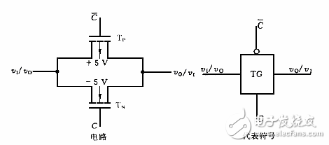
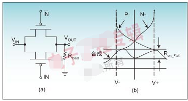
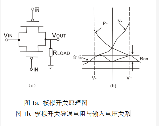
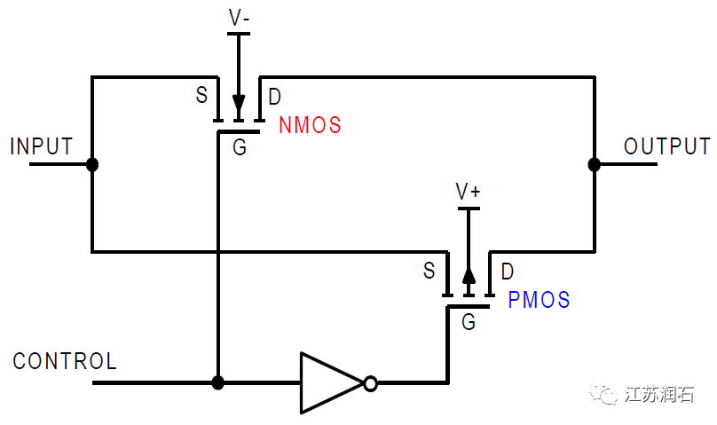
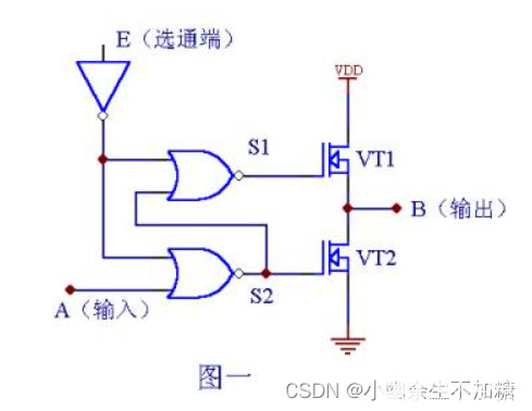
When the voltage on node A is a Logic 1, the complementary Logic 0 is applied to node active-low A, allowing both transistors to conduct and pass the signal at IN to OUT. When the voltage on node active-low A is a Logic 0, the complementary Logic 1 is applied to node A, turning both transistors off and forcing a high-impedance condition on both the IN and OUT nodes. This high-impedance condition represents the third "state" (high, low, or high-Z) that the DS3690 channel may reflect downstream.
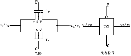
The schematic diagram (Figure 1) includes the arbitrary labels for IN and OUT, as the circuit will operate in an identical manner if those labels were reversed. This design provides true bidirectional connectivity without degradation of the input signal.

Figure 1. Schematic representation of a transmission gate.
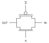
The common circuit symbol for a transmission gate depicts the bidirectional nature of the circuit's operation (Figure 2).
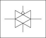
Figure 2. Circuit symbol.
The connection scheme in Figure 3 is designed to isolate the I/O bus between the microprocessor and the memory component, in case the memory is removed. The SRAM is physically mounted on a removable memory card; the DS3690 transmission gate is used to isolate the various signals routed through the connector.

Figure 3. Typical DS3690 application circuit.
The ground connection from the SRAM is fed back through the connector to pull down the DS3690 Chip Enable (active-low CE) pin. This action enables the transmission gate when the memory card is installed.
Using the TQFN package, all signals can be conveniently routed in the physical direction of the bus. Finally, for convenience and application flexibility, the designer decides the assignment of a signal to one of the DS3690's 26 channels.
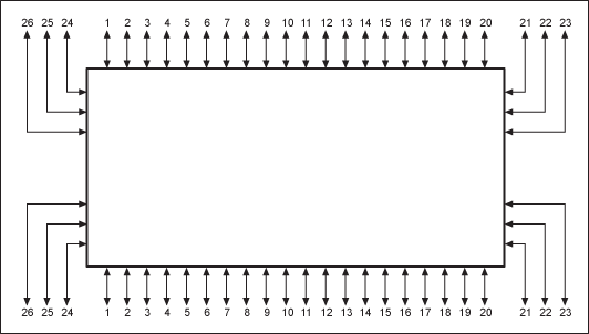
Figure 4. Suggested signal routing.
Basic Operation
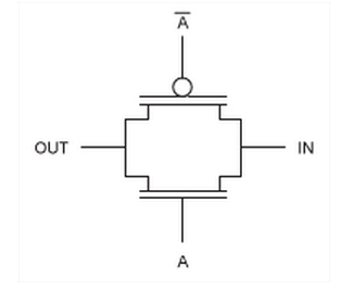
A transmission gate, or analog switch, is defined as an electronic element that will selectively block or pass a signal level from the input to the output. This solid-state switch is comprised of a pMOS transistor and nMOS transistor. The control gates are biased in a complementary manner so that both transistors are either on or off.When the voltage on node A is a Logic 1, the complementary Logic 0 is applied to node active-low A, allowing both transistors to conduct and pass the signal at IN to OUT. When the voltage on node active-low A is a Logic 0, the complementary Logic 1 is applied to node A, turning both transistors off and forcing a high-impedance condition on both the IN and OUT nodes. This high-impedance condition represents the third "state" (high, low, or high-Z) that the DS3690 channel may reflect downstream.
The schematic diagram (Figure 1) includes the arbitrary labels for IN and OUT, as the circuit will operate in an identical manner if those labels were reversed. This design provides true bidirectional connectivity without degradation of the input signal.

Figure 1. Schematic representation of a transmission gate.
The common circuit symbol for a transmission gate depicts the bidirectional nature of the circuit's operation (Figure 2).

Figure 2. Circuit symbol.
What Are Transmission Gates Used for?
Transmission gates are typically used as building blocks for logic circuitry, such as a D Latch or D Flip-Flop. As a stand-alone circuit, a transmission gate can isolate a component or components from live signals during hot insertion or removal. In a security application, they can selectively block critical signals or data from being transmitted without proper hardware-controlled authorization.The connection scheme in Figure 3 is designed to isolate the I/O bus between the microprocessor and the memory component, in case the memory is removed. The SRAM is physically mounted on a removable memory card; the DS3690 transmission gate is used to isolate the various signals routed through the connector.

Figure 3. Typical DS3690 application circuit.
The ground connection from the SRAM is fed back through the connector to pull down the DS3690 Chip Enable (active-low CE) pin. This action enables the transmission gate when the memory card is installed.
What Is So Unique About the DS3690?
High Number of Independent Channels Reduces Component Count
The DS3690, with 26 independent channels, has the highest bus width available on the market today. Most commercially available transmission gates are configured to accommodate 2, 4, or 8 discrete signals. Using the Figure 3 example, this SRAM requires 25 discrete signals to be isolated when the card is removed. Using conventional 8-bit transmission gates, the designer would have to place four separate components to isolate this SRAM, significantly increasing the final component count and dedicated PC-board area.Small Package Saves Board Space
The DS3690 is packaged in a 5mm x 11mm TQFN, requiring a mere 55mm2 of PC-board area for this entire bus-isolation effort. If the designer had selected 8-bit transmission gates, the most aggressive packaging available is an SSOP that occupies 51.5mm2 each. Given a minimal allowance for signal routing, the four 8-bit components would occupy well over 200mm2 to accomplish the same function as a single DS3690.Efficient Signal Routing for Better Performance
The additional board area required for multiple 8-bit components also complicates the PC-board layout effort: dissimilar trace lengths can result in dissimilar signal skew on critical timing events. Additionally, the four 8-bit components selected may not have identical propagation delays, further aggravating the operational margin of the final system. The DS3690's 26 parallel data channels (Figure 4) result in no more than 1ns of channel-to-channel deskew.Using the TQFN package, all signals can be conveniently routed in the physical direction of the bus. Finally, for convenience and application flexibility, the designer decides the assignment of a signal to one of the DS3690's 26 channels.

Figure 4. Suggested signal routing.
 電子發燒友App






評論