Abstract: This application note shows a reference design using the MAX15026 low-cost, high-efficiency synchronous buck converter in an auxiliary power supply for LCD TVs or set-top boxes. This reference design generates a 5V, 5A power supply from a wide, 6.5V to 24V input voltage range.
Key specifications for the reference design are listed below, along with a detailed schematic (Figure 1) and the bill of materials (Table 1) needed for this application.
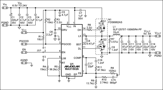
Figure 1. Schematic of the MAX15026 synchronous buck converter for a 300kHz switching frequency.
Table 1. Bill of Materials
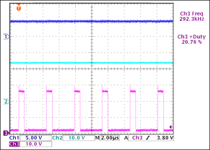
Figure 2. Steady-state output voltage, input voltage, and switching-node voltage at VIN = 24V, VOUT = 5V.
Ch1: VOUT; Ch2: VIN; Ch3: Lx Node Voltage
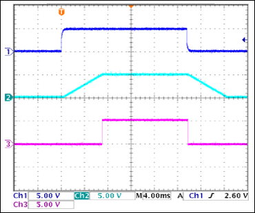
Figure 3. Enable, soft-start, soft-stop and PGOOD sequence waveforms.
Ch1: Enable; Ch2: VOUT; Ch3: PGOOD
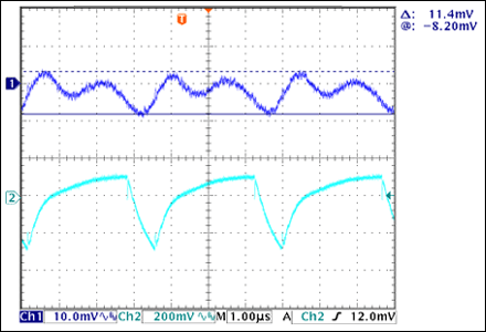
Figure 4. Output and input ripples at VIN = 24V, VOUT = 5V and IOUT = 5A.
Ch1: Output Voltage Ripple; Ch2: Input Voltage Ripple
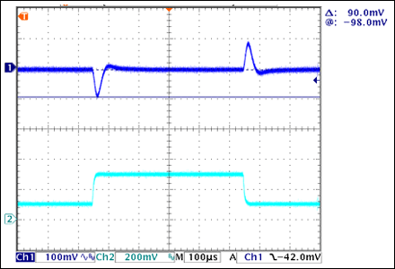
Figure 5. Converter load transient response with a 2A step change in load current.
Ch1: Output Voltage Dip; Ch2: Load-Step Change (1A/div)
Load Current Step Change: 1A to 3A
Load Current Slew Rate: 2A/μs
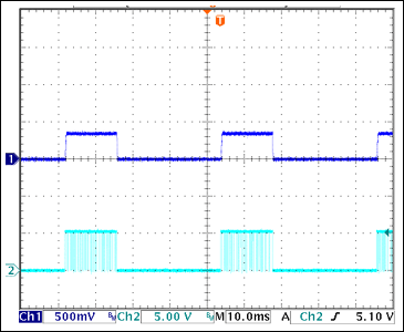
Figure 6.Hiccup-mode overcurrent protection with output shorted.
CH1: Output Voltage; CH2: Gate Pulses
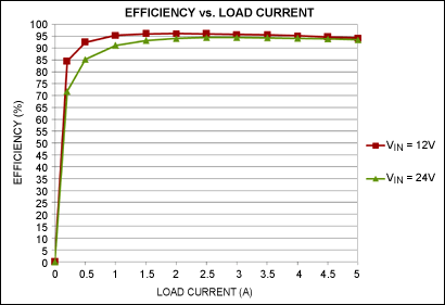
Figure 7. Efficiency vs. load current plots.
Key specifications for the reference design are listed below, along with a detailed schematic (Figure 1) and the bill of materials (Table 1) needed for this application.
Specifications
- Input Voltage Range: 6.5V to 24V
- Output Voltage: 5V
- Output Current: 5A
- Output Voltage Ripple (pk-pk): 50mV
- Switching Frequency of Converter: 300kHz
- Overcurrent Protection Limit: 6A
- Efficiency: > 90% for Normal Operation

Figure 1. Schematic of the MAX15026 synchronous buck converter for a 300kHz switching frequency.
Table 1. Bill of Materials
| Designator | Value | Description | Part | Footprint | Manufacturer | Quantity |
| C1 | 220μF, 35V | Capacitor | EEVFK1V221P | 8mm x 10.2mm | Panasonic | 1 |
| C2, C3 | 4.7μF, 50V | Capacitor | GRM31CR71H475KA12L | 1206 | Murata | 2 |
| C4 | 0.1μF, 50V | Capacitor | GRM188R71H104KA93D | 0603 | Murata | 1 |
| C5 | 4.7μF, 6.3V | Capacitor | GRM188R60J475KE19D | 0603 | Murata | 1 |
| C6 | 2.2μF, 6.3V | Capacitor | GRM188R60J225KE19D | 0603 | Murata | 1 |
| C7 | 1μF, 50V | Capacitor | GRM21BR71H105KA12L | 0805 | Murata | 1 |
| C8 | 0.47μF, 16V | Capacitor | GRM188R71C474KA88D | 0603 | Murata | 1 |
| C9, C16 | 1200pF, 50V | Capacitor | GRM1885C1H122JA01D | 0603 | Murata | 2 |
| C10, C11 | 47μF, 10V | Capacitor | GRM32ER71A476KE15L | 1210 | Murata | 2 |
| C12, C13, C14 | 22μF, 10V | Capacitor | GRM31CR71A226KE15L | 1206 | Murata | 3 |
| C15 | 560pF, 50V | Capacitor | GRM1885C1H561JA01D | 0603 | Murata | 1 |
| C17 | 22pF, 50V | Capacitor | GRM1885C1H220JA01D | 0603 | Murata | 1 |
| R1 | 10Ω | Resistor | SMD 1% Resistor | 0603 | Vishay | 1 |
| R2 | 10kΩ | Resistor | SMD 1% Resistor | 0603 | Vishay | 1 |
| R3, R6 | 2.2Ω | Resistor | SMD 1% Resistor | 0603 | Vishay | 2 |
| R4 | 15kΩ | Resistor | SMD 1% Resistor | 0603 | Vishay | 1 |
| R5 | 56.2kΩ | Resistor | SMD 1% Resistor | 0603 | Vishay | 1 |
| R7 | 3.57Ω | Resistor | SMD 1% Resistor | 1206 | Vishay | 1 |
| R8 | 102kΩ | Resistor | SMD 1% Resistor | 0603 | Vishay | 1 |
| R9 | 13.7kΩ | Resistor | SMD 1% Resistor | 0603 | Vishay | 1 |
| R10 | 2.74kΩ | Resistor | SMD 1% Resistor | 0603 | Vishay | 1 |
| R11 | 47.5kΩ | Resistor | SMD 1% Resistor | 0603 | Vishay | 1 |
| L1 | 10μH ±20%, 5.5A | Inductor | SLF12575T-100M5R4-PF | 12.5mm x 12.5mm x 7.5mm | TDK | 1 |
| N1 | 30V, 6.3A, 35.5mΩ—Q1; 30V, 8.6A, 16.5mΩ—Q2 |
Dual MOSFET | FDS6982AS | 8-SO | Fairchild | 1 |
| U1 | PWM Controller | Low-Cost, DC-DC Synchronous Buck Controller with a 4.5V to 28V Operating Range | MAX15026BETD+ | 14-TDFN-EP | Maxim | 1 |
Performance Data

Figure 2. Steady-state output voltage, input voltage, and switching-node voltage at VIN = 24V, VOUT = 5V.
Ch1: VOUT; Ch2: VIN; Ch3: Lx Node Voltage

Figure 3. Enable, soft-start, soft-stop and PGOOD sequence waveforms.
Ch1: Enable; Ch2: VOUT; Ch3: PGOOD

Figure 4. Output and input ripples at VIN = 24V, VOUT = 5V and IOUT = 5A.
Ch1: Output Voltage Ripple; Ch2: Input Voltage Ripple

Figure 5. Converter load transient response with a 2A step change in load current.
Ch1: Output Voltage Dip; Ch2: Load-Step Change (1A/div)
Test Conditions
VIN = 12V, VOUT = 5VLoad Current Step Change: 1A to 3A
Load Current Slew Rate: 2A/μs

Figure 6.Hiccup-mode overcurrent protection with output shorted.
CH1: Output Voltage; CH2: Gate Pulses

Figure 7. Efficiency vs. load current plots.
 電子發燒友App




評論