| Technology Family | AXC |
| Applications | UART, JTAG |
| Bits (#) | 2 |
| High input voltage (Min) (Vih) | 0.45 |
| High input voltage (Max) (Vih) | 3.6 |
| Vout (Min) (V) | 0.65 |
| Vout (Max) (V) | 3.6 |
| IOH (Max) (mA) | -12 |
| IOL (Max) (mA) | 12 |
| Rating | Automotive |
- AEC-Q100 automotive qualified
- Fully configurable dual-rail design allows each port to operate with a power supply range rrom 0.65 V to 3.6 V
- Operating temperature from –40°C to +125°C
- DIR control input for each channel
- Glitch-free power supply sequencing
- Up to 380 Mbps support when translating from 1.8 V to 3.3 V
- VCC isolation feature
- If either VCC input is below 100 mV, all I/O outputs are disabled and become high-impedance
- Ioff supports partial-power-down mode operation
- Compatible with AVC-family level shifters
- Latch-up performance exceeds 100 mA per JESD 78, class II
- ESD protection exceeds JEDEC JS-001
- 8000-V Human-body model
- 1000-V Charged-device model
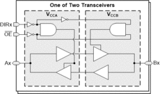
The SN74AXC2T245-Q1 is a two-bit noninverting bus transceiver that uses two individually configurable power-supply rails. The device is operational with both VCCA and VCCB supplies as low as 0.65 V. The A port is designed to track VCCA, which accepts any supply voltage from 0.65 V to 3.6 V. The B port is designed to track VCCB, which also accepts any supply voltage from 0.65 V to 3.6 V. Additionally the SN74AXC2T245-Q1 is compatible with a single-supply system.
The SN74AXC2T245-Q1 device is designed for asynchronous communication between data buses. The device transmits data from the A bus to the B bus or from the B bus to the A bus, depending on the logic level of the direction-control inputs (DIRx). The SN74AXC2T245-Q1 device is designed so the control pin (DIR) is referenced to VCCA.
This device is fully specified for partial-power-down applications using the Ioff current. The Ioff protection circuitry ensures that no excessive current is drawn from or to an input, output, or combined I/O that is biased to a specific voltage while the device is powered down.
The VCC isolation feature ensures that if either VCCA or VCCB is less than 100 mV, both I/O ports enter a high-impedance state by disabling their outputs.
Glitch-free power supply sequencing allows either supply rail to be powered on or off in any order while providing robust power sequencing performance.


